Shenzhen Pengsheng MicroVision Tech Co., Ltd.
Silicon-based Micro-OLED displays are poised for significant market growth[1].
Omdia, a market research firm, states that Micro LED, silicon-based LED, and silicon-based OLED are expected to account for about 5% of the total display panel market by 2031[2].
According to statistics from CINNO Research, the compound annual growth rate (CAGR) of the global AR/VR silicon-based OLED display panel market from 2021 to 2025 will reach 119%, with the market size expected to hit $1.47 billion in 2025[3].
What are the fundamental technologies of silicon-based Micro-OLED? How did these technologies emerge? This article provides an in-depth look at the seven fundamental technologies of silicon-based Micro-OLED displays.
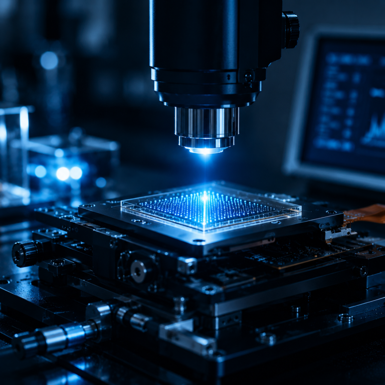
1. Single-Crystalline Silicon Substrate Technology
In silicon-based Micro-OLEDs, the single-crystalline silicon substrate serves as a stable platform for circuit integration. This substrate features exceptional planarity and material uniformity[4].
In subsequent manufacturing processes, this flat platform ensures high reliability for technological upgrades.
Moreover, it forms the basis for the miniaturization of silicon-based Micro-OLEDs and is ideal for precisely manufacturing tiny, complex circuit structures.
In the next decade, the processing of single-crystalline silicon substrates will become more refined to achieve smaller form factors. This relies on advanced lithography technology to fabricate tiny transistors and circuits.
In addition, manufacturing processes such as chemical vapor deposition (CVD) are continually driving down costs, making these products more accessible globally.
Scientists are making improvements to further reduce defect density and production overhead.
2. CMOS Driver Circuit Integration Technology
CMOS (Complementary Metal-Oxide-Semiconductor) is the backbone of modern integrated circuits, though it was historically not applied in display manufacturing.
However, with the mass adoption of VR technology, CMOS driver circuit integration is gradually being applied to Micro-OLED production.
In silicon-based Micro-OLEDs, tens of millions of transistors are integrated on the substrate to form the CMOS driver circuit. These circuits precisely control the brightness and color of each pixel[5].
For example, in silicon-based Micro-OLEDs using active matrix (AM) driving, each pixel is controlled by an independent transistor, resulting in ultra-low latency and high refresh rates.
In the future, new CMOS driver circuits will optimize signal paths, reduce impedance, and further shorten latency. Additionally, the use of extreme ultraviolet lithography (EUV) will further reduce chip size and defect rates.
3. OLED Organic Material and Luminescence Technology
Silicon-based Micro-OLEDs require high-efficiency luminescent organic materials, categorized into hole transport, electron transport, and luminescent layers.
For example, Micro-OLEDs using phosphorescent organic materials can utilize both singlet and triplet excitons, significantly boosting luminous efficiency.
The luminescence in these displays is based on the principle of electroluminescence. Microcircuits generate an electric field, triggering a series of complex physical phenomena that generate photons through exciton radiative transitions[6].
4. Micro-Nano Processing Technology
Leveraging advanced lithography, etching, and thin-film deposition, silicon-based Micro-OLEDs achieve high resolution within a compact size.
This gives silicon-based Micro-OLEDs a competitive edge in microscopy, medicine, and near-eye display devices.
For example, in VR hardware, small and lightweight Micro-OLEDs mitigate wearer fatigue. These lighter devices significantly improve the user experience, encouraging daily use.
With the continuous progress of lithography, the pixel size of silicon-based Micro-OLEDs has the potential for further reduction, achieving even higher resolutions.
5. Organic Material Encapsulation Technology
Since OLED organic materials are highly susceptible to moisture and oxygen, resulting in performance degradation, encapsulation is required to isolate them from the environment.
Currently, the most common methods include glass cover encapsulation and Thin-Film Encapsulation (TFE).
TFE deposits a thin film directly on the OLED surface to form a barrier layer. Because TFE is thinner and more flexible, it is better suited for silicon-based Micro-OLEDs[7].
Some flexible displays use this method to enable curling, which is essential for the manufacturing of flexible-screen smartphones.
6. Microlens Array (MLA) Technology
The luminous efficiency of silicon-based Micro-OLEDs is easily affected by external factors.
Microlens Array (MLA) technology improves luminous efficiency and ensures uniform light distribution. Microlenses function by focusing and collimating light.
Engineers install microlenses above the luminescent layer to create an array that directs light toward the viewer, making the display image more consistent and bright.
7. Silicon-based Micro-OLED Displays:Anti-Ambient Light Reflection Technology
To reduce the reflection of sunlight and ambient light, silicon-based Micro-OLEDs employ anti-reflection and anti-glare technologies.
Scientists apply an anti-reflection coating to the display surface, drastically reducing reflectivity and minimizing ambient light interference, allowing for a much clearer viewing experience.
References:
- Goldman Sachs Equity Research. (2024). The Rise of Micro-OLED in the Spatial Computing Era.
- Omdia. (2023). Display Long-term Demand Forecast Tracker – 2023 Analysis.
- CINNO Research. (2024). Global AR/VR Silicon-based OLED Market Analysis and Forecast 2021-2025.
- Vogel, U., et al. (2022). “Micro-OLED on Silicon: A Review of CMOS-Integrated Displays.” Journal of the Society for Information Display (JSID).
- IEEE Xplore. (2023). “Advanced CMOS Backplane Design for High-Resolution Micro-OLED Displays.” Proceedings of the International Electron Devices Meeting (IEDM).
- Nature Communications. (2023). “High-efficiency Phosphorescent Organic Light-Emitting Diodes for Near-Eye Displays.”
- S.W. Lee, et al. (2023). “Advanced Thin-Film Encapsulation (TFE) for Next-Generation Micro-Displays.” Advanced Materials Interfaces.