

For next-generation near-eye displays such as AR and VR, RGB Micro‑OLED stands out as the premier technical path that delivers both high brightness and high power efficiency. By eliminating color filters (CF), it avoids the ~70% light loss inherent to filter-based architectures, enabling dramatic gains in luminous efficacy and brightness even at ultra-high resolutions.
Nevertheless, low-cost mass production of RGB Micro‑OLED remains an immense challenge. Extreme pixel density requirements and stringent alignment tolerances have long bottlenecked its commercial rollout. The microdisplay industry has for years been dominated by white OLED plus color filter (WOLED) designs, largely because no direct evaporation tool could previously achieve micron-level alignment precision. Apple Vision Pro, for example, relies on Sony-supplied silicon-based OLED (OLEDoS) microdisplays with exceptional resolution, yet these still use the WOLED + color filter stack and suffer from fundamental light absorption losses in the filter layer.
Canon Tokki, the leading display equipment manufacturer based in Niigata, Japan, has now revealed a landmark development at SID Display Week 2026: a high-PPI evaporation system built for 12-inch wafers. The system achieves wafer-to-mask alignment accuracy of ±0.1 μm, breaking long-standing process constraints and delivering a viable mass-production hardware platform for high-efficiency RGB Micro‑OLED panels.
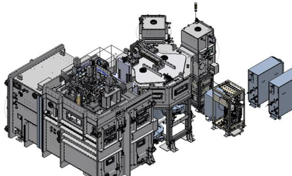
I. Why Direct RGB Micro‑OLED Evaporation Is So Challenging
Commercially available Micro‑OLED panels today range from 0.5 to 2 inches diagonal and typically exceed 3000 PPI. The prevailing WOLED workflow leverages mature, high-yield white OLED deposition paired with color filters, but the filters sap a large share of emitted light and cap overall efficiency.
Legacy deposition tools also lack sufficient alignment performance. G6H glass OLED mass-production evaporators hit roughly ±3 μm alignment error, while WOLED evaporation systems for Micro‑OLED often fall between ±10 μm and ±100 μm — far below the required specification. The core barrier to filter-free RGB patterning is precise micron-scale registration and intimate contact between the pixel pattern and the fine metal mask (FMM).
II. Core Technical Breakthrough: Four Hardware Enablers for ±0.1 μm Ultra-High Precision
To hit the ±0.1 μm target, Canon Tokki integrated four foundational technologies into the new 12-inch evaporation platform:
- Magnetically levitated motion stage Silicon wafers are held by electrostatic chucks on the maglev stage, isolating the substrate from mechanical vibration. Silicon is infrared-transparent, so IR cameras capture alignment marks from the wafer backside. This registers the wafer to the mask without damaging the emissive layers.
- Mask tilt tracking mechanism High-resolution FMMs are brittle and prone to cracking on contact. This module pre-scans and compensates for angular misalignment between substrate and mask before they make contact.
- Soft-contact alignment assembly It brings the substrate and mask into gentle contact while supporting nanometer-scale lateral fine positioning. This maximizes conformal contact, minimizes the gap between surfaces, suppresses evaporation shadowing and prevents pixel cross-talk.
- Empirical precision validation Metrology shows 3σ alignment error of 34.7 nm under non-contact conditions. Even in the magnet-clamped operational state with the mask secured, alignment holds at 36.8 nm.
III. Architectural Advantages of the 12-inch RGB Evaporation Prototype
Independent mask transport architecture
Conventional OLED evaporators share the same robotic transfer path for silicon wafers and FMMs. Repeated organic deposition residue builds up on masks, raising the risk of pixel shorting and yield loss. Canon Tokki’s prototype fully segregates mask and wafer transport lines. Mask exchange chambers are clustered and interfaced with mask cleaning hardware to cut contamination and substantially boost panel yield.
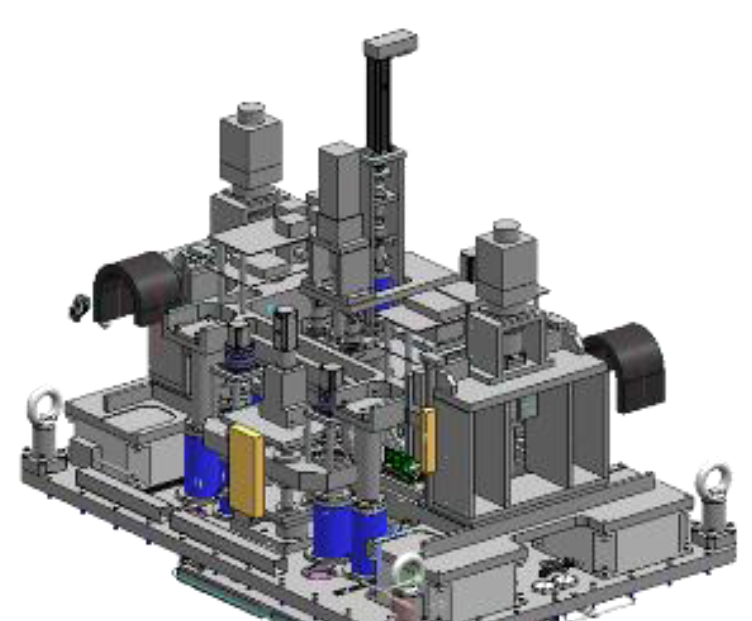
Linear evaporation source scanning
The linear scanning source design lowers chamber height, improves organic material utilization, curtails equipment capital cost and dampens vibration-induced precision drift. It also simplifies vacuum pumping infrastructure and reduces the build expense of these large vacuum systems. Compared with conventional broad-area diffuse emission, directional scanning through the FMM drastically improves consumption efficiency of costly organic emissive materials.
High-PPI masks and device coupons
The team has fabricated electroplated metal masks rated for 3000 PPI and continues development toward 5000 PPI masks. Functional patterned RGB emissive devices at 3200 PPI have been successfully demonstrated. In the conceptual multi-chamber serial production layout, the target tact time is approximately 4 minutes per 12-inch wafer.
IV. R&D Progress Across the Industry
Samsung Display and LG Display both showed high-brightness RGB OLEDoS prototypes for AR/VR around SID 2026. Even so, cost hurdles have kept these designs out of volume consumer end products.
Separately, some specialist vendors can produce small batches of native RGB OLEDoS microdisplays such as the 0.39-inch, 3386 PPI variant reaching 60,000 nits. These are mostly deployed in defense systems, premium industrial and electronic viewfinder (EVF) hardware, plus engineering evaluation units for leading AR developers.
Roadblocks Ahead for RGB Micro‑OLED Mass Commercialization
While the prototype has validated critical process workflows, Canon Tokki notes two persistent bottlenecks: immature high-resolution mask manufacturing and elevated system build cost. A premium custom vacuum evaporator of Canon Tokki’s caliber carries a price tag of hundreds of millions of RMB, and silicon CMOS backplane tapeout adds further overhead. The upfront capital expenditure (CapEx) remains substantial. Widespread adoption will require coordinated innovation across the entire microdisplay supply chain to bring ultra-high-resolution RGB Micro‑OLED to market.
References
- Masahiro Ichihara. (2026). Development of the 12-inch High-ppi Deposition System. SID International Symposium Digest of Technical Papers (SID 2026 Proceedings), San Jose, CA.
- Society for Information Display (SID). (2026). OLED Microdisplay Technology Roadmap and Direct-Emission RGB OLEDoS Progress. SID Display Week 2026 Market Insights & Trends Report.
- Display Supply Chain Consultants (DSCC). (2025/2026). AR/VR Display Technologies and Market Outlook: OLEDoS vs. Micro-LED. DSCC Quarterly Micro-Display Shipment and Technology Report.
- Samsung Display & LG Display. (2026). Next-Generation High-Brightness RGB OLEDoS Prototypes for AR/VR Applications. Technical Presentation at SID 2026 Exhibition & Symposium.
- Omdia. (2025/2026). Micro-Display Equipment Landscape: The Role of High-Precision Vacuum Deposition in FMM OLEDoS Manufacturing. Omdia Display Equipment Market Tracker.
- TrendForce. (2026). Analysis of High-Resolution FMM and Silicon-Based Mask Technologies for 3000+ PPI OLEDoS. TrendForce AR/VR Industry Research Brief.
- Apple Inc. / Sony Semiconductor Solutions. (2023–2026). Technical Architecture of Silicon-Based OLED Microdisplays in Spatial Computing Devices. IEEE / SID Technical Documentation & Product teardown analysis.
- International Electrotechnical Commission (IEC) & SEMI Standards. (2025). Measurement Methods and Terminology for Micro-Displays in Augmented and Virtual Reality. SEMI / IEC Joint Technical Committee Report.