Shenzhen Pengsheng MicroVision Tech Co., Ltd.




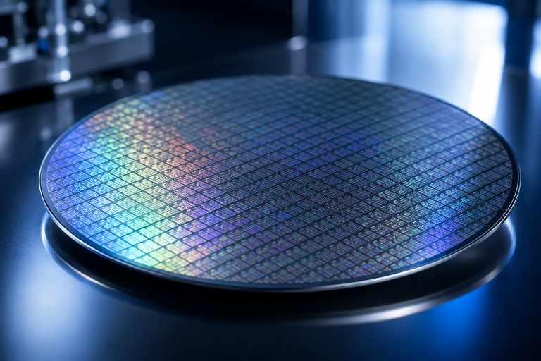
Among the latest microdisplay technologies, micro-OLED has become the flagship display solution for Apple Vision Pro XR headsets, owed primarily to its ultra-high PPI. Silicon-based OLEDoS (micro-OLED) panels feature minuscule pixel dimensions, delivering crisp visuals free of the screen-door effect even when viewed up close by users.
That said, an unbreakable physical constraint persists across the display industry: the higher the PPI of a micro-OLED panel, the more difficult it is to boost its peak brightness, measured in nits. Take the standard Sony-manufactured panel inside Apple Vision Pro as an example. Each eye is paired with a 1.42-inch display that hits a sustained full-screen peak brightness of only 1,000 nits, with a typical continuous operating brightness ranging from 200 to 300 nits. To accommodate densely packed pixels, the silicon backplane is covered with driving circuits and isolation trenches, resulting in an extremely low pixel aperture ratio. Most of each pixel’s real estate is occupied by circuitry and light-blocking layers, leaving only a tiny fraction dedicated to actual light emission.
This tradeoff stems from a complex interplay of semiconductor physics, light outcoupling efficiency, and fundamental material limits.

1. Sharply Reduced Aperture Ratio: Shrinking Light-Emitting Zones
The single biggest factor limiting brightness in high-PPI micro-OLEDs is a drastically cut aperture ratio. The aperture ratio refers to the percentage of a single pixel’s total area dedicated to light emission.
When PPI climbs from 1,000 to over 4,000, tens of millions of subpixels must be crammed onto a one-inch wafer, compressing the overall pixel footprint to an extreme degree. While pixels shrink down, isolating barriers, routing traces, and signal crosstalk prevention gaps cannot be scaled down proportionally without bound.
The end result: denser pixel layouts equal smaller aperture ratios. With identical driving current supplied, less surface area available for light emission inherently dims the display output.
The mass-production panel for Apple Vision Pro illustrates this clearly. It boasts a 3,387 PPI rating with a 7.5 μm pixel pitch. Microscopic teardown testing reveals driving traces, light-shield barriers, and silicon thin-film transistors take up 72% of each pixel, leaving just 28% as the light-emitting aperture (an aperture ratio of 28%). For this reason, a balanced performance sweet spot caps sustained full-screen brightness at 1,000 nits, with routine daily use limited to 200–300 nits.
2. Electrical and Optical Crosstalk Plus Leakage Risks
At multi-thousand PPI densities, subpixels sit mere micrometers—or even sub-micrometers—apart from one another.
At such extreme compactness, the high anode voltages required for bright output trigger electrical leakage between adjacent pixels. Cranking up drive current artificially causes unintended illumination of neighboring subpixels, introducing color shifts and degraded contrast. Optical crosstalk emerges as a secondary issue: light emitted by one subpixel refracts diagonally into adjacent pixel zones.
A useful counterpoint is Sony’s electronic viewfinder (EVF) panels for cameras, built on 1,800 PPI OLEDoS with a 14 μm pixel pitch. The ample spacing between subpixels nearly eliminates leakage and optical crosstalk, enabling a native stable brightness of 2,000 nits.
To mitigate crosstalk of both varieties, micro-OLED manufacturers are forced to cap the maximum drive current per pixel, hard-setting an upper limit on brightness—a necessary compromise with no easy workaround.
3. Light Loss in the WOLED + Color Filter Architecture
Nearly all mass-producible micro-OLED panels capable of exceeding 3,000 PPI rely on the white OLED plus color filter (WOLED + CF) manufacturing route.
This design generates uniform white light from a base emissive layer, then filters the output through overlaying red, green, and blue (RGB) color filters to produce distinct hues.
Unfortunately, color filters inherently incur massive optical losses. Over 70% of incoming white light gets absorbed by the filter stack, with less than 30% transmitted through to the viewer.
At higher PPI values, each individual color filter subpixel shrinks further, exacerbating light blocking and scattering while dragging down overall light outcoupling efficiency.
4. The Thermal and Lifespan Paradox
Silicon backplanes outperform traditional glass substrates in thermal conductivity, yet they endure severe thermal stress at ultra-high PPI ratings. Tightly clustered emissive nodes trap heat and drive panel temperatures sharply upward. Forced current increases to chase brighter output send heat generation soaring exponentially, shortening overall device lifespan.
Compounding this issue, OLED organic emissive materials are highly temperature-sensitive. Prolonged exposure to elevated heat accelerates material degradation, triggering permanent brightness decay and color drift. To guarantee a commercial service life of tens of thousands of hours, manufacturers must compromise on power draw and maximum brightness levels.
Industry Breakthroughs: Future Solutions for High-PPI, High-Brightness Micro-OLEDs
As outlined above, current micro-OLED suppliers rely on careful performance balancing, yet this approach carries inherent limitations. To resolve this core tradeoff, leading global microdisplay developers are advancing three transformative cutting-edge technologies:
- Micro Lens Array (MLA) An additional refractive lens layer is deposited atop the color filter stack. MLAs redirect stray angled light rays back toward the viewer, boosting light outcoupling efficiency by over 50% without raising power consumption. Sony integrated this light extraction technology—including micro-lens structures—into its 1.3-inch per-eye 4K micro-OLED panels supplied to Apple Vision Pro. Paired with the WOLED+CF stack, this design pushes native peak brightness to 3,000–5,000 nits.
- Tandem OLED Stack Architecture Two or more emissive layers are vertically stacked with charge generation layers (CGLs) in between. At identical current densities, tandem structures deliver double the light output, easing material strain in high-PPI configurations.
- Native RGB Self-Emissive Micro-OLED (Filter-Free Design) Native RGB self-emissive micro-OLED represents the industry’s long-term end goal. Abandoning the WOLED+CF workflow entirely, it uses high-precision fine metal masks (FMM) or excimer laser lift-off to pattern independent red, green, and blue organic emissive pixels. Eliminating color filter light loss unlocks theoretical peak brightness levels ranging from several thousand to over ten thousand nits.
At the end of 2023, Samsung Display made a major strategic acquisition of U.S. microdisplay pioneer eMagin, securing exclusive rights to its proprietary dPd™ technology. At CES 2026, Samsung Display showcased its latest native RGB silicon-based OLEDoS microdisplays built on this platform.
Conclusion
Today’s micro-OLED technology faces an inherent balancing act between pixel density (PPI) and brightness, constrained by usable emissive area and unavoidable optical losses. With MLA and tandem stacking optimizations, commercial micro-OLED panels now deliver effective in-view brightness of 2,000 to 3,000+ nits. Looking ahead, native RGB self-emissive micro-OLED technology will fully dismantle this historic brightness-density tradeoff.
References:
[1] Engadget. Apple Vision Pro teardown uncovers pixels the size of red blood cells[EB/OL]. 2024.
[2] Sony Semiconductor Solutions. OLED Microdisplay Technical Overview[EB/OL]. Sony Official Product Portal.
[3] Apple Inc. Apple Vision Pro Official Technical Specifications[EB/OL].
[4] Shin H J, Kim Y D, Choi B D. 4670‐PPI OLEDoS pixel circuit design for wide data voltage range in a 0.13 μm CMOS process[C]//SID Symposium Digest of Technical Papers, 2024. Quantifies electrical leakage & optical crosstalk at sub-7 μm pixel pitches; explains mandatory drive current limitation to suppress color distortion.
[5] Abeeluck A K, et al. 4032 ppi High-resolution OLED microdisplay[C]//SID Symposium Digest, 2018. 4032 PPI high-density prototype test data: shrinking aperture ratio drastically cuts native luminance without MLA light extraction.
[6] Haas G. Microdisplays for augmented and virtual reality – OLED vs LED Based Systems[C]//SID Symposium Digest, 2019. Systematic comparison of WOLED+CF light loss, silicon backplane thermal stress, fundamental PPI-brightness physical constraints for XR microdisplays.
[7] Park et al. Performance evaluation of micro lens arrays: Improvement of light intensity and efficiency of white organic light emitting diodes[J]. PLOS ONE, 2022, 17(6).
[8] ACS Photonics Team. Waveguide Mode Outcoupling in Deep-Stacked White OLEDs Using a Subelectrode Microlens Array[J]. ACS Photonics, 2026.
[9] Zhao J W, et al. P-256: Research on the High-Temperature Lifetime Stability of Tandem Devices[C]//SID Symposium Digest, 2025.
[10] Qian Y Z, et al. Power consumption of light engines for emerging augmented reality glasses: perspectives and challenges[J]. Advanced Photonics, 2025, 7(3).
[11] eMagin Corporation. Direct Patterning (dPd™) Microdisplay Technology Whitepaper[EB/OL].
[12] Ghosh A, et al. Developing the World’s Brightest WUXGA OLED Microdisplay[C]//SID Symposium Digest, 2022.
[13] Samsung Display. CES 2026 RGB Silicon OLEDoS Microdisplay Presentation Deck, 2026. Post-acquisition eMagin dPd™ mass-production roadmap; industry endgame for breaking the PPI-brightness tradeoff cycle.
About the Author
Leo Harrison has over a decade of experience in the East Asian display supply chain and display semiconductor industry, specializing in smart hardware architecture and display technology evaluation.
Review Team
Review Team:
Special technical review and engineering validation provided by the Pengsheng Technology R&D Division.