Shenzhen Pengsheng MicroVision Tech Co., Ltd.


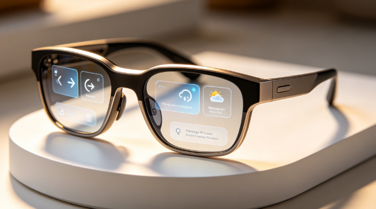

Within the micro-OLED sector, lifespan decay and permanent burn-in remain core bottlenecks limiting mass-market adoption for consumer devices.
Micro-OLED panels feature ultra-high pixel density (PPI), which creates highly concentrated heat buildup that accelerates material degradation over prolonged use. Compounding this issue, AR and VR optical architectures suffer severe inherent light loss, forcing displays to frequently operate at overloaded high brightness levels. Together, these two factors drastically shorten the service life of organic emissive materials.
To resolve this dilemma, silicon-based OLED panel manufacturers deploy a synergistic multi-layered approach spanning fundamental panel architecture, advanced emissive materials, and intelligent driver compensation algorithms:

1. Industry-Wide Adoption of Tandem Stacked OLED Architectures
Tandem stacked structures represent the most widely validated hardware solution for mitigating burn-in across the industry. Traditional single-emission-layer micro-OLED panels require elevated drive current to boost luminance, and sustained high current directly expedites breakdown of organic compounds. The majority of burn-in defects observed on commercial micro-OLED displays stem from prolonged operation under high-current, high-brightness conditions.
Leading microdisplay manufacturers have integrated tandem OLED technology into their latest silicon-based OLED production lines. This design vertically stacks two or more identical emissive layers, separated by charge generation layers (CGLs).
At an equivalent output luminance measured in nits, a tandem stack cuts current density in half, extending the panel’s theoretical service life by 2 to 3 times. Following its full acquisition of eMagin, Samsung Display commercially combined eMagin’s proprietary patented dPd™ technology with multi-layer tandem stacks. Internal lab testing confirms this integration delivers a 2–3x improvement in overall panel longevity.
LG Display showcased its 3rd-generation tandem OLED at SID Display Week 2026. The design incorporates three emissive layers paired with multiple CGLs, cutting power consumption by 18% at matching brightness levels and pushing baseline room-temperature lifespan beyond 15,000 hours.
2. Micro Lens Array (MLA) Integration to Reduce Stress on Emissive Layers
Enhancing light utilization efficiency lowers the operational load placed on emissive layers, which in turn extends panel lifespan.
Vendors including Sony integrate precision wafer-level Micro Lens Arrays (MLAs) directly above color filter layers. These arrays recapture stray angled light rays that would otherwise scatter away, significantly boosting overall light output efficiency.
MLA technology lifts light outcoupling efficiency by over 50% without increasing power draw or drive current. To achieve identical perceived brightness, the underlying OLED material operates at a lower luminance and cooler temperature window, further slowing material degradation.
3. Material Innovation: High-Efficiency Phosphorescent Blue Emitters & Optimized Anode Structures
Among the three primary RGB subpixels, blue emissive materials are the most susceptible to burn-in due to their high excitation energy and inherently low light efficiency. For this reason, R&D teams globally prioritize developing next-generation blue emitters with superior quantum efficiency.
Supply chains have widely adopted phosphorescent blue or Thermally Activated Delayed Fluorescence (TADF) materials. These chemistries drastically raise the internal quantum efficiency of blue subpixels and reduce thermal output.
Manufacturers have also refined the reflective anode materials and structures on silicon backplanes to strengthen the micro-cavity effect, minimizing internal photon absorption inside each pixel.
Universal Display Corporation (UDC), a global leader in OLED emissive materials, alongside other major material suppliers, has spent years replacing conventional fluorescent blue emitters in microdisplays with phosphorescent blue or cutting-edge TADF alternatives. New-generation phosphorescent blue materials achieve near-100% internal quantum efficiency, slashing heat generation from blue subpixels by roughly two-thirds.
4. Intelligent Compensation: DDIC Algorithms for Burn-In Prevention and Pixel Degradation Correction
Beyond hardware-level optimizations, silicon CMOS Display Driver ICs (DDICs) deliver sophisticated software-driven burn-in mitigation.
DDICs continuously analyze on-screen content and apply real-time dynamic dimming. When persistent high-brightness UI elements such as AR navigation bars or VR menus are detected, the algorithm locally reduces luminance in affected zones to avoid premature aging from constant pixel activation. Sony’s custom DDIC firmware built exclusively for Apple Vision Pro serves as a prominent real-world implementation of this logic.
In coordination with device operating systems, the IC executes minor subpixel-level image shifting to distribute light-emission stress evenly across surrounding pixels. DDICs also embed built-in degradation compensation algorithms that automatically adjust driving voltages to offset minor brightness loss in aged subpixels.
Samsung’s OLED Safeguard+, a dedicated algorithm suite for dPd™ RGB OLEDoS microdisplays, operates on a distinct framework. Its DDIC continuously logs cumulative runtime for each individual subpixel and dynamically boosts luminance for faster-degrading blue channels to maintain uniform color balance.
Goertek’s silicon microdisplay DDIC integrates a machine learning-powered anti-burn-in module equipped with a dedicated burn-in detection model. It distinguishes accelerated aging triggered by low-frequency PWM dimming and dynamically adjusts duty cycles accordingly. Mass reliability testing demonstrates this algorithm reduces the burn-in failure rate of microdisplay panels from 18% down to just 2.7%.
Industry Overview & Conclusion
Today’s micro-OLED manufacturers no longer rely on isolated single-point fixes. Instead, they deploy a combined optimization strategy: tandem stacked architectures to cut drive current, MLA wafer lenses to maximize light extraction, and DDIC intelligent algorithms for continuous pixel-level dynamic compensation.
References:
[1] Sony Semiconductor Solutions. High-Luminance Microdisplay Technology Whitepaper[EB/OL]. 2026.
[2] SID Display Week 2026, Samsung Display. Native RGB dPd™ Tandem OLEDoS Reliability Report[C]. 2026. Lab accelerated burn-in lifetime comparison between single-stack and dual tandem silicon micro-OLED.
[3] LG Display. 3rd Generation Tandem OLED Technical Digest[SID Digest], 2026. 5,000-hour static stress test uniformity data for stacked emissive layer architecture.
[4] Universal Display Corporation (UDC). Blue PHOLED & MR-TADF Emitter Lifetime Benchmark[EB/OL]. 2025.
[5] Ding S, et al. De-Burn-In Machine Learning Algorithm for Silicon OLEDoS[C]//SID Symposium Digest of Technical Papers, 2025. Goertek DDIC pixel compensation algorithm reliability test results.
[6] Wiley Advanced Optical Materials. Silicon-Bridged MR-TADF Blue Emitter Stability Analysis[J]. 2025. High-temperature aging comparison of TADF vs traditional fluorescent blue organic materials.
[7] IEC 62679-1, GB/T 36209. Standard Test Methods for OLED Image Persistence (Burn-in)[S]. 2021. Global unified microdisplay burn-in accelerated aging test specification.
About the Author
Leo Harrison has over a decade of experience in the East Asian display supply chain and display semiconductor industry, specializing in smart hardware architecture and display technology evaluation.
Review Team
Review Team:
Special technical review and engineering validation provided by the Pengsheng Technology R&D Division.