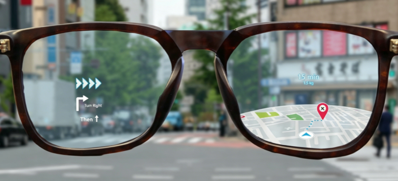

Hailed as the ultimate display technology of the 21st century, Micro-LED boasts promising market prospects. Nevertheless, its commercial rollout faces a major bottleneck in mass manufacturing: mass transfer, an engineering challenge pushing the boundaries of present-day physics. This constraint yields low production yields and exorbitant manufacturing costs, hindering widespread commercial adoption.
In conventional display fabrication, light-emitting layers and driver backplanes are built concurrently. For Micro-LED manufacturing by contrast, wafer epitaxial growth and panel backplane processing are entirely decoupled. Mass transfer refers to the process of accurately, damage-free and high-speed placing millions to billions of micro-chips smaller than 50 µm from their growth substrate onto a display backplane — a feat that conveys the immense technical difficulty involved.
What Are Micro-LED’s Advantages? Comparison of Mainstream Display Technologies
| Technology | Chip / Pixel Size | Emission Mechanism | Material System | Core Bottlenecks |
| LCD | No discrete micro-chips | Backlight-modulated light blocking | Liquid crystal + organic color filters | Poor contrast, high power consumption |
| OLED | No discrete micro-chips | Self-emissive | Organic compounds | Burn-in susceptibility, limited peak brightness |
| Mini-LED | 100 – 200 µm | Backlight local dimming | Inorganic GaN | Thick form factor, poor suitability for micro-displays |
| Micro-LED | < 50 µm (scalable below 10 µm) | Self-emissive | Inorganic GaN | Mass transfer and yield repair |
Root Causes Behind Micro-LED Mass-Production Difficulties
Micro-LED manufacturing demands an uncommon combination of ultra-high throughput, sub-micrometer placement accuracy and near-perfect yield.
- Speed constitutes one critical limitation. A 4K television features over 24.9 million RGB sub-pixels. Conventional mechanical pick-and-place or flip-chip bonding would take dozens of days to process a single panel, resulting in prohibitive costs.
- Accuracy represents a second major hurdle. Once chip dimensions shrink below 20 µm, van der Waals and electrostatic forces overpower gravity. Mechanical nozzles can pick up chips yet fail to reliably place them.
- Yield requirements are extraordinarily stringent. For a Full-HD (1920 × 1080) panel with fewer than five dead pixels permitted, pixel yield must reach 99.9999%. Even minuscule failure probabilities stemming from wafer-growth defects or transfer-induced damage scale into catastrophic reject rates when multiplied across tens of millions of pixels.
These constraints impose extreme process requirements, translating directly to the formidable cost of Micro-LED volume manufacturing.
Laser Lift-Off (LLO) and Laser-Induced Forward Transfer (LIFT)
To overcome physical limits of mechanical transfer, vendors such as 3D-Micromac have developed laser-based solutions.
- Laser Lift-Off (LLO): UV nanosecond lasers operating within the 193–355 nm spectrum pass through the transparent sapphire substrate. The GaN interfacial layer absorbs laser energy, rapidly heating to roughly 900 °C and undergoing photothermal decomposition to generate nitrogen gas and liquid gallium. This micro-explosion at the interface detaches chips en bloc from the substrate, while the sapphire substrate may be recycled.
- Laser-Induced Forward Transfer (LIFT): LIFT does not etch chips directly. Instead, laser energy acts as a precision propulsion source. A donor substrate is aligned face-down toward the target substrate. A flat-top laser beam passes through a transparent intermediate layer to heat the chip’s backside. Vapourisation-induced local impulse releases chips, which land precisely at designated positions.
- Achieving Ultra-High Yields: Laser-driven mass-transfer platforms such as 3D-Micromac’s microCETI adopt a dual-track strategy to mitigate yield constraints. Transfer throughput reaches approximately 130 million chips per hour, substantially lowering per-panel manufacturing costs. Placement accuracy lies below 2 µm, supporting today’s 20–50 µm chips while providing margin for next-generation sub-10 µm ultra-fine devices. Combined with photoluminescence (PL) and electroluminescence (EL) inspection for defect screening, LIFT’s selective single-chip transfer capability enables removal of defective dies and precise replacement with known-good chips. This closed-loop production workflow pushes realised yield toward the 99.9999% target.
Q&A
- Q1: What differentiates Micro-LED from Mini-LED and OLED?
- A1: Micro-LED is a self-emissive display technology featuring chips smaller than 50 µm. It delivers finer pixel pitches than Mini-LED. While both Micro-LED and OLED are self-emissive, Micro-LED employs inorganic GaN, delivering superior brightness and reliability. Its primary manufacturing obstacle lies in mass transfer of micro-scale chips.
- Q2: What is mass transfer, and why is it the principal bottleneck for Micro-LED mass production?
- A2: Mass transfer is the process of rapidly and accurately transferring and bonding millions to billions of Micro-LED chips from a donor substrate onto a display backplane. A Full-HD panel contains millions of pixels and demands 99.9999% yield. Traditional mechanical pick-and-place and serial flip-chip bonding cannot satisfy production throughput requirements, rendering mass transfer the central constraint on Micro-LED manufacturing cost.
- Q3: How does LIFT laser-transfer technology work?
- A3: LIFT (Laser-Induced Forward Transfer) applies controlled laser energy to heat the interface between chips and the donor substrate. Chips detach from the donor and travel to target positions. The laser functions as an energy trigger rather than a conventional material-processing tool, supporting selective transfer of single or multiple chips.
References
- Is Micro LED Better Than OLED? A Deep-Dive Comparison (Micro LED vs OLED), 2026 — Pengsheng Tech
- Mini LED, Micro LED & OLED: Complete Display Technology Breakdown, 2026 — Pengsheng Tech
- Mass transfer techniques for large-scale and high-density microLED arrays, International Journal of Extreme Manufacturing, 2022. (Review covering mass-transfer fundamentals, mechanical vs laser transfer, yield requirements)
- Achieving High-Throughput MicroLED Manufacturing with LIFT, Journal of the Society for Information Display, 2023.
- Heterogeneous integration of micro-LEDs via multiple simultaneous transfer and bonding, Science Advances, 2026.
- Direct laser transfer and thermocompression bonding process of blue GaN micro-LED arrays, Applied Physics Letters, 2025. (LLO / laser transfer GaN chip mechanism, UV-laser-driven interface decomposition)
- Full-Process Detection Technologies for Micro-LED Advanced Manufacture, Research, 2026. (PL / EL inspection, bad-die repair, closed-loop yield improvement workflow)
Legal Disclaimer
This white-paper is intended solely for technical reference and does not constitute clinical guidance, engineering consultancy, procurement advice or regulatory counsel. All trademarks and product names are property of their respective owners. Technical-performance descriptions are based on publicly available vendor documentation and third-party industry analysis. Real-world clinical outcomes depend on full system integration, clinical workflows and regulatory validation. Readers must independently verify all performance metrics, colour-calibration requirements and regulatory compliance obligations prior to any medical-device implementation. No express or implied warranty is given for completeness or accuracy of content herein.