Shenzhen Pengsheng MicroVision Tech Co., Ltd.




The Screen Door Effect (SDE): A Major Immersion Killer for VR & AR Headsets
The screen door effect (SDE) ranks among the most disruptive visual flaws that ruin immersion in VR and AR eyewear.
What Is SDE on Silicon-Based Micro OLED Displays?
Simply put, the screen door effect describes a grid of fine black lines overlaying your field of view, as if you were viewing content through a mesh screen. For years, this optical artifact stood as a critical roadblock holding back mass-market consumer VR adoption. Take the era of the HTC Vive and Oculus Rift as an example: early glass-based panels only delivered an aperture ratio of 25% to 40%. This meant 60% to 75% of the visible display area consisted of dark pixel gap lines.
| Hardware Model | Panel Substrate & Type | PPI | Per-Eye Resolution | Aperture Ratio | Pixel Gap Scale | PPD | Screen Door Effect Severity |
|---|---|---|---|---|---|---|---|
| Original HTC Vive | Glass-substrate OLED | 447 | 1080×1200 | ~35% | Micrometer (μm) | ~11 | Severe; grainy, sand-like pixelation |
| Meta Quest 2 | Glass-substrate LCD | 773 | 1832×1920 | ~60% | Micrometer (μm) | ~20 | Noticeable; heavy jagged edges on text |
| Meta Quest 3 | Premium Glass LCD | 1218 | 2064×2208 | ~70% | Micrometer (μm) | ~25 | Faint; prominent against solid-color backgrounds |
| Apple Vision Pro | CMOS Silicon-Based Micro OLED | ~3386 | 3660×3200 | >90% | Nanometer (nm) | ~40–45 | Virtually imperceptible; print-like seamless imagery |
This breakdown dissects the root causes of the screen door effect and its drastically reduced visibility on silicon-based Micro OLED panels.

1. Defining the Screen Door Effect & Its Root Cause
OLED imagery is rendered by countless tiny red, green, and blue subpixels. During silicon-based Micro OLED manufacturing, gaps between pixels are reserved for wiring and drive circuitry—these circuit zones emit no light.
When viewing standard smartphones or televisions, the viewing distance to the panel is far enough that these minuscule black gaps blend into the background and go unnoticed by human vision.
VR/AR hardware flips this dynamic entirely: the display sits mere centimeters from the user’s eyes, paired with high-magnification optical eyepieces. These lenses magnify the tiny dark pixel gaps to starkly visible black grids, creating the sensation of peering through a mesh screen and severely degrading visual immersion—this is the screen door effect.
2. Core Metrics for Quantifying SDE: PPI and PPD
To understand how silicon-based Micro OLED solves this flaw, two key display metrics must first be clarified:
- PPI (Pixels Per Inch): The physical pixel density of a display panel.
- PPD (Pixels Per Degree): The number of pixels visible to the human eye within one degree of field of view.
The display industry widely accepts that the human eye’s maximum resolving threshold sits at roughly 60 PPD. Any headset with a PPD rating below 60 will reveal distinct black pixel grids, resulting in obvious screen door distortion. Manufacturers therefore aim to push device PPD above the 60 PPD threshold.
Legacy VR headsets relying on glass-substrate LCD/OLED panels only reach 700–1200 PPI, translating to approximately 20 PPD at best. SDE remains glaringly obvious, with jagged, frayed edges on all on-screen text.
3. How Silicon-Based Micro OLED Eradicates the Screen Door Effect
Silicon-based Micro OLED reimagines display manufacturing from the ground up, fundamentally eliminating the screen door artifact via four core advancements:
3.1 Manufacturing Overhaul: Silicon Wafer Substrates
Conventional panels use LTPS circuitry printed onto glass substrates. Glass imposes hard physical limitations on fabrication precision, leaving no room to shrink pixel gaps further.
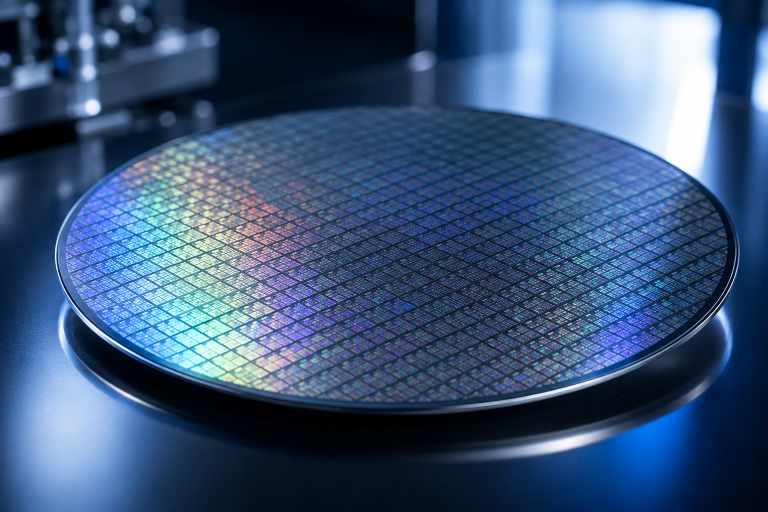
Silicon-based Micro OLED panels are fabricated directly on monocrystalline silicon wafers, leveraging the same high-precision photolithography processes used to mass-produce CPUs and semiconductors. This technology shrinks inter-pixel spacing to unprecedented minuscule dimensions.
Sony’s monocrystalline silicon Micro OLED chips for XR hardware adopt mature 28 nm / 55 nm semiconductor wafer lithography. The pixel pitch of these panels is reduced to 7.8 micrometers, with dark inter-pixel gaps compressed down to the hundreds-of-nanometers scale.
3.2 Order-of-Magnitude PPI Surge (3,000–4,500+ PPI)
Ultra-high fabrication precision shrinks individual pixel dimensions to just several micrometers, pushing panel pixel density to 3,000–4,500+ PPI. When paired with custom optical eyepieces, headsets equipped with these panels hit 50–60+ PPD, edging right up against the human eye’s native resolution limit.
3.3 Aperture Ratio Boost Exceeding 90%
Traditional displays cram light-emitting pixels and drive circuitry onto a single flat plane. The more space allocated to wiring, the less surface area remains for luminous subpixels—resulting in wide, dark non-emissive gaps.
Silicon-based Micro OLED utilizes a vertical 3D stacked architecture: the bottom layer houses dense CMOS drive circuitry, while the entire top layer functions exclusively as the OLED light-emitting layer. Circuitry is tucked beneath the pixel array, lifting aperture ratios above 90%.
3.4 Optical Refinement with Micro-Lens Arrays (MLA)
Flagship silicon-based Micro OLED devices such as Apple Vision Pro integrate a micro-lens array (MLA) atop the emissive layer. Each individual subpixel sits beneath a micrometer-scale convex lens that concentrates light output for enhanced brightness, while leveraging light refraction and dispersion to deliver smoother, more uniform visuals.
Additionally, Japan’s research institute SEL debuted an innovative Micro OLED solution at Display Week that resolves high-brightness power consumption and luminance decay pain points. Its ultra-high-density 4,200 PPI panel hits 10,000 nits without MLA integration; pairing the panel with an MLA pushes peak brightness all the way to 20,000 nits.
Conclusion
The screen door effect refers to visible black grid lines formed by magnified gaps between display pixels under high-power VR/AR optics. Silicon-based Micro OLED eliminates this flaw by harnessing semiconductor photolithography to achieve ultra-dense pixel layouts, paired with a 3D stacked design that conceals drive circuitry under the light-emitting layer for aperture ratios above 90%.
References:
[1] SeeYA Technology Whitepaper: 3D Stacked Architecture and Aperture Ratio Optimization for Silicon-Based Micro OLED Microdisplay Chips
[2] Society for Information Display (SID) Technical Paper: Angular Resolution (PPD) and Human Visual Thresholds in Near-Eye Display (NED) Systems
[3] Sony Semiconductor Solutions Datasheet: ECX344A Series: Technical Analysis of 55 nm Process Micro-Lens Array (MLA) Silicon-Based Micro OLED
[4] Samsung Display × eMagin Joint Press Release: dPd™ Direct Patterning Technology: Progress on Filter-Free RGB 5,000 PPI Micro OLED for Next-Generation High-Brightness AR/VR
About the Author
Leo Harrison has over a decade of experience in the East Asian display supply chain and display semiconductor industry, specializing in smart hardware architecture and display technology evaluation.
Review Team
Review Team:
Special technical review and engineering validation provided by the Pengsheng Technology R&D Division.