Shenzhen Pengsheng MicroVision Tech Co., Ltd.

Transparent Micro-OLED displays represent a groundbreaking innovation in display technology developed in recent years.
The technology was first engineered in August 2024 by the Milestone Lab at Germany’s Fraunhofer Institute for Photonic Microsystems (IPMS). The team delivered the world’s first CMOS silicon-based transparent Micro-OLED with 45% transmittance, debuting a fully functional, drivable prototype at South Korea’s IMID 2024 exhibition. As the first transparent Micro-OLED microdisplay with viable commercialization potential, it is engineered exclusively for near-eye display applications in AR glasses.
This wave of technological innovation is fueled by exponentially surging market demand. Industry projections forecast the global transparent display market will expand explosively from a $6 billion valuation in 2025 at a compound annual growth rate (CAGR) of 45.0%.
A well-documented bottleneck for display fabrication on silicon wafers is silicon’s inherent opacity paired with extremely dense wiring layouts. Prior to this breakthrough, research institutions including Fraunhofer, eMagin, and China’s Olightek had only produced small-scale transparent silicon-based OLED samples with transmittance below 20%. These prototypes suffered from poor light penetration and insufficient brightness, remaining confined to academic research papers without real-world deployment.
Quantitative Comparison: Core Specs vs. Large-Scale Transparent OLED Panels
Data is sourced from leading industry research publications, including Future Market Insights 2025/2026 reports and SID Display Week datasets. Silicon-based transparent microdisplays differ fundamentally from glass-substrate large transparent panels used in subway window screens and transparent televisions:
| Key Feature | Conventional Large-Scale Transparent OLED (Glass TFT Substrate) | Transparent Micro-OLED (Silicon CMOS / OLEDoS Substrate) |
|---|---|---|
| Flagship Product Example | LG SIGNATURE OLED T (77-inch transparent TV) | Fraunhofer IPMS Milestone Prototype (0.5–1.3 inches) |
| Pixel Density (PPI) | 100–150 PPI (noticeable pixel grain when viewed up close) | 3,000–4,500+ PPI (retina-grade clarity, eliminates screen door effect) |
| Pixel Pitch | Hundreds of micrometers (μm) | Below 10 micrometers (μm) |
| Overall Transmittance | 38%–45% | Industry-first 45% (theoretical maximum exceeds 50%) |
| Response Time | Millisecond (ms) scale | Microsecond (μs) scale (virtually zero motion blur, reduces AR-induced motion sickness) |
| Primary Limitations | Oversized form factor; incompatible with lightweight portable hardware | Extremely complex manufacturing, low production yields, high unit costs |
What Are Transparent Micro-OLED Displays?
Simply defined, they integrate two cutting-edge technologies: transparent display architecture and Micro-OLED (silicon-based OLEDoS) microdisplays. The panels deliver glass-like light transmission alongside chip-level ultra-high pixel density.
Core Technology Behind Transparent Micro-OLED Displays
1. Miniaturization: Silicon Wafer-Driven OLEDoS Architecture
Conventional OLED panels for smartphones and televisions rely on glass TFT substrates, with pixel densities generally capped at 300–500 PPI. Micro-OLED abandons glass entirely, using single-crystal silicon wafers—the identical material used to manufacture computer semiconductors—as its base layer. This design shrinks individual pixels down to micrometer dimensions, enabling pixel densities of 3,000 to over 4,000 PPI. To put this in perspective, a surface no larger than a fingernail can house a full 2K or even 4K resolution panel.
2. Achieving Transparency: Optimized Cathode & Substrate Design
Radical material and structural overhauls are required to render these high-density silicon chips transparent. Manufacturers discard conventional opaque metal anodes and cathodes, replacing them with ultra-thin light-permeable nanomaterials such as ITO or ultra-thin silver-magnesium alloy.
At the microstructural level, dedicated fully transparent light transmission zones are integrated alongside RGB light-emitting subpixels to allow unobstructed light passage. The result is a panel that resembles lightly tinted glass when powered off, while projecting floating digital imagery layered over real-world surroundings when activated.
Engineers employ plasma dry etching to strip organic materials from the transparent light transmission zones, requiring precise iterative tuning of plasma power and gas mixture ratios. Insufficient etching leaves micrometer-thick organic residue, triggering severe light dispersion and an unwanted rainbow effect. Over-etching, by contrast, bombards and permanently damages the underlying CMOS passivation layer, ruining the silicon chip entirely.
Two Dominant Technical Development Routes
- Pixel Gap Architecture: Drive circuitry and wiring are drastically miniaturized to carve fully transparent voids between micrometer-scale RGB subpixels.
- Cluster Array Architecture: Pixels are grouped into compact display clusters, with wide transparent channels separating each cluster. A monolithically integrated microlens array (MLA) is bonded directly to the chip surface, precisely focusing display light toward the user’s eyes while ambient external light passes unimpeded through transparent channels.
Material science advancements further minimize light absorption and reflection:
Fully reflective anodes are eliminated in electrode redesigns, replaced with nanoscale ultra-thin silver/magnesium alloy or ITO as shared semi-transparent top electrodes. Production workflows eliminate residual OLED organic layers, while nanometer-thick anti-reflective coatings (ARCs) are deposited on panel surfaces to cut internal interface reflectivity to a minimum.
3. Core Competitive Advantages of Transparent Micro-OLED Displays
Compared with large-format transparent OLED panels (transparent televisions, subway window screens):
| Feature | Conventional Transparent OLED (Glass Substrate) | Transparent Micro-OLED (Silicon Substrate) |
|---|---|---|
| Pixel Density (PPI) | 100–150 (visible pixel grain) | 3,000+ (ultra-smooth, noise-free visuals) |
| Display Size Range | Dozens to over one hundred inches | Typically 0.5–1.5 inches |
| Brightness & Contrast | Low performance, easily washed out by ambient light | Exceptional metrics; self-emissive pixels deliver infinite contrast ratio |
| Response Speed | Millisecond scale | Microsecond scale (near-total elimination of motion blur) |
4. Primary Application Scenarios for Transparent Micro-OLED Displays
Their compact footprint, ultra-high resolution, and light transmittance—paired with elevated production costs—rule out use in household living room televisions. Instead, this technology serves as the foundational hardware for next-generation near-eye displays, with use cases including but not limited to:
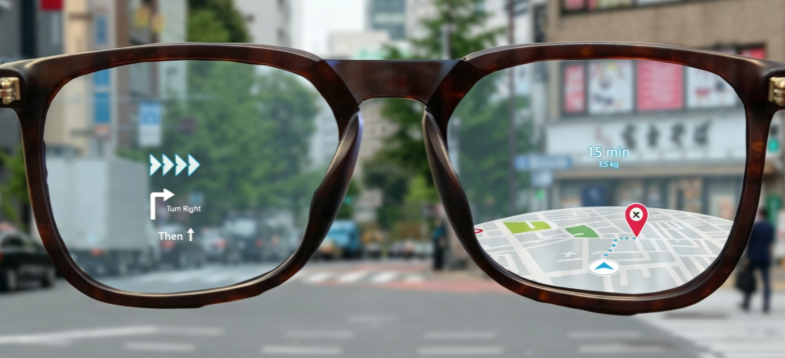
- AR Smart Glasses: Traditional AR eyewear relies on optical waveguides to refract ambient light, while transparent Micro-OLED can be integrated directly into lens substrates. Wearers maintain unobstructed sight of real-world environments while viewing navigation markers, live translation text, or mobile notification overlays.
- Automotive Head-Up Displays (HUDs): Embedded within vehicle windshields or rearview mirrors, they overlay speed readouts and ADAS driving-assistance visuals onto the road ahead without obstructing the driver’s line of sight.
- Premium Miniature Optical Instruments: Night vision goggles, microscopes, compact rangefinders, and scopes. Users observe physical subjects while viewing real-time digital thermal imaging data and measurement calibration markers superimposed within their field of view.
5. Current Unresolved Technical Barriers
While commercial prospects remain promising, transparent Micro-OLED production sits in the early-to-mid industrialization phase due to extremely complex manufacturing workflows, hindered by the following core limitations:
Increasing panel transmittance requires expanding light passage zones, which shrinks the surface area available for light-emitting pixels and suppresses overall brightness. Boosting luminance for outdoor use, conversely, demands partial sacrifices to light transmittance.
Additionally, packing ultra-high pixel density onto tiny silicon chips generates substantial heat under peak load. Balancing high peak brightness with low power consumption remains an active R&D priority for manufacturers including Sony and BOE.
Wafer fabrication plants worldwide cite unresolved contamination defects during mass transfer as their most critical production hurdle. Micrometer-scale dust particles trapped between substrate layers disable dozens of surrounding pixels, rendering entire panel sections non-functional.
Reference Sources
[1] Fraunhofer IPMS Official Press Release (2024). Transparent Electronics: 45 Percent Transparency achieved in Microdisplays. Official technical disclosure documenting the prototype presented at IMID 2024 by Germany’s Fraunhofer Institute for Photonic Microsystems.
[2] IMID 2024 Conference Proceedings. High-Transmittance OLEDoS Development under the HOT Project. Exhibition abstract detailing the 45% transmittance silicon microdisplay developed under Project HOT (Grant No. MAVO 840092) at Korea’s International Meeting on Information Display.
[3] Photonics Spectra (2024). Transparency Gains Characterize Fraunhofer OLED Microdisplays. In-depth industry analysis outlining the Pixel Approach and Cluster Array development frameworks.
[4] Journal of the Society for Information Display (JSID). Monolithic Integration of Microlens Arrays on Silicon-Based Micro-OLEDs for Efficiency Enhancement. Theoretical research validating microlens arrays as a solution to limited light-emitting surface area and improved forward light extraction efficiency.
[5] IEEE Photonics Technology Letters. Dry Etching Optimization for Clear Apertures in Transparent Organic Light-Emitting Devices. Process research exploring plasma dry etching workflows to clear organic layers in transparent zones and mitigate the rainbow optical artifact.
[6] Thin Solid Films. Nanometer-scale Ultra-thin Ag/Mg Alloy Films and ITO as Semi-transparent Top Electrodes for OLEDoS. Core materials science paper covering semi-transparent shared top electrodes and anti-reflective coating (ARC) design.
[7] IEC 63145-10 International Standard. Eyewear display — Part 10: Generic specification and test methods for augmented reality glasses. Global IEC standard outlining testing protocols for transmittance and image ghosting on AR near-eye hardware.
[8] Future Market Insights (FMI) 2025/2026 Industry Report. Global Transparent Display Market Analysis and Forecast (2025–2035). Market dataset predicting 45.0% CAGR growth across large glass-based and silicon microdisplay transparent panels.
[9] DSCC (Display Supply Chain Consultants) Whitepaper. The Evolution of OLEDoS: From Apple Vision Pro to Next-Generation Transparent AR Glasses. Industrialization roadmap detailing power efficiency, thermal management, and mass transfer yield optimization from leading silicon microdisplay manufacturers Sony and BOE.
[10] SID Display Week Technical Digest. Tandem Structure and Advanced Passivation Layers in Silicon-Based Micro-Displays. Compiled core technical research from the Society for Information Display addressing high-load thermal buildup and passivation layer anti-erosion protection for silicon microdisplays
About the Author
Leo Harrison has over a decade of experience in the East Asian display supply chain and display semiconductor industry, specializing in smart hardware architecture and display technology evaluation.
Review Team
Review Team:
Special technical review and engineering validation provided by the Pengsheng Technology R&D Division.