Shenzhen Pengsheng MicroVision Tech Co., Ltd.
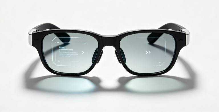

As high-end spatial computing devices, digital surgical head-mounts, and thermal imaging optics push microdisplay technology into the global spotlight, display components now account for one of the largest single line items in a device’s Bill of Materials (BOM), trailing only high-performance compute chips and memory [1].
To the untrained eye, a display seems like a thin sheet of emissive glass. However, when shrinking a display down to the size of a fingernail (0.23″ to 1.31″), the underlying physics and engineering move out of conventional panel manufacturing and straight into advanced semiconductor microelectronics fabrication [2].
This article provides an in-depth analysis of Micro-OLED (OLED on Silicon / OLEDoS) manufacturing costs, technical bottlenecks, CMOS backplate economics, and the global supply chain landscape—alongside practical strategies for OEMs to optimize display integration [1], [3].
💡 Key Insights (TL;DR)
- Semiconductor Evolution: Micro-OLED is not simply a miniature traditional OLED; it merges silicon CMOS wafer fabrication with organic OLED evaporation [2].
- Primary Cost Drivers: Expense is driven by high 12-inch CMOS wafer backplate foundry fees, Tandem WOLED + CF (Color Filter) light-efficiency losses, and initial mass-production yield rates hovering between 30% and 50% [1], [4].
- Market Consolidation: Sony and SeeYA collectively account for over 80% of global XR Micro-OLED panel shipments, while companies like BOE, Samsung Display, and specialized integration partners are expanding capacity [1], [5].
- Turnkey Integration: Partnering with specialized supply chain integrators—such as Shenzhen Pengsheng MicroVision Technology Co., Ltd.—allows enterprise clients to mitigate R&D risks by acquiring integrated display, driver board, and optical module solutions [3].
1. Technical Clarification: Micro-OLED (OLEDoS) vs. Micro-LED (LEDoS)
A common point of confusion in near-eye display (NED) procurement is conflating Micro-OLED with Micro-LED. Although both aim for high pixel density (PPI), they represent distinct material physics and manufacturing paths [2], [6].
- Micro-OLED (OLED on Silicon / OLEDoS): Employs organic small-molecule light-emitting layers vacuum-deposited directly onto a single-crystal silicon CMOS wafer backplate [2]. It is the most commercially mature solution for high-density VR/MR headsets, electronic viewfinders (EVF), medical AR, and optical sights [1], [4].
- Micro-LED (LEDoS / Glass-based Micro-LED): Uses inorganic Gallium Nitride (GaN) or Indium Gallium Nitride (InGaN) micro-chips transferred onto a TFT glass or silicon substrate via mass transfer [6]. It remains in early commercialization due to mass transfer yield barriers, inspection/repair complexity, and full-color challenges [3], [6].
| Feature / Metric | Micro-OLED (Silicon-based OLED) | Micro-LED (LEDoS / Glass-based) |
| Emissive Material | Organic small-molecule layers [2] | Inorganic semiconductor dies (GaN/InGaN) [6] |
| Substrate / Backplate | Single-Crystal Silicon CMOS Wafer (8″/12″) [2] | Glass TFT or Silicon CMOS Substrate [6] |
| Colorization Method | White OLED + Color Filter (WOLED + CF) [4] | RGB Chip Mass Transfer or Blue + QDCC [6] |
| Pixel Density (PPI) | 3,000 to 7,000+ PPI [1] | 1,000 to 10,000+ PPI [6] |
| Contrast Ratio | >1,000,000:1 [4] | >1,000,000:1 [6] |
| Primary Cost Bottlenecks | CMOS Wafer cost, Evaporator depreciation, CF loss [1] | Mass transfer yield, micro-repair, RGB full color [6] |
| Primary Target Applications | VR/MR, Medical AR, Thermal Sights, EVF, Smart Helmets [4] | Ultra-bright Outdoor AR Waveguides, Automotive HUD [3] |
2. Breakdown: Why Are Micro-OLED Displays So Expensive?
Standard 0.49-inch Micro-OLED panels during initial production runs typically range from 30 to 40 USD per unit, while large-format 1.31-inch high-resolution panels can exceed 150 to 200 USD in BOM allocation [1], [5]. The underlying expense is tied to four critical hardware layers:
Micro-OLED Cost Structure Breakdown
├── 1. CMOS Silicon Wafer Backplate (~35% - 45%)  -> Advanced foundry process fees & die area limits
├── 2. OLED Evaporation & Organic Layers (~20% - 25%) -> Tandem multi-stack materials & vacuum tooling
├── 3. Color Filter (CF) & Photolithography (~15% - 20%) -> Chip-scale sub-pixel RGB alignment
└── 4. Packaging, Testing & Optics (~10% - 15%)   -> Wafer dicing, glass encapsulation & optical bonding
1) The CMOS Wafer Backplate: Transitioning from Glass to Silicon
Traditional display panels use amorphous silicon (a-Si) or LTPS TFT on glass substrates, priced per square meter [2]. Micro-OLED utilizes single-crystal silicon wafers (CMOS Wafer) as the driving backplate [2], [4].
- Foundry Wafer Cost: Manufacturing moves from 8-inch wafers (0.18 um / 0.11 um processes) to 12-inch wafers (55 nm / 40 nm nodes) [1]. A single processed 12-inch CMOS wafer costs thousands of dollars from semiconductor foundries [1]. Because wafer area is physically limited, larger panel sizes (e.g., 1.31-inch vs. 0.39-inch) yield drastically fewer functional display dies per wafer [1], [5].
- Integrated Sub-Pixel Circuitry: To achieve over 4,000 PPI within a display the size of a postage stamp, complex pixel driving circuits, threshold voltage compensation, and high-speed interfaces (MIPI/LVDS) are embedded directly into the silicon wafer, elevating the backplate cost to that of a custom IC [2].
2) Light Efficiency Loss: The WOLED + CF Architecture
The most viable full-color Micro-OLED manufacturing process uses White OLED with a Color Filter (WOLED + CF) array [4].
Tandem Architecture: To achieve high luminance and acceptable operational lifespan, manufacturers deploy a multi-stack Tandem WOLED structure (stacking multiple organic emissive layers vertically) [4]. However, when broad-spectrum white light passes through the RGB Color Filter, over 70% of the light energy is absorbed or reflected [4].
To overcome this photometric loss, displays require higher driving currents and additional organic layers, extending processing time inside high-vacuum evaporation equipment (e.g., Canon Tokki systems) and raising material consumption costs [1], [4].
3) Yield Rate Curves: The 30%–50% Mass Production Hurdle
Unlike mature TV and smartphone LCD/OLED panels that enjoy yield rates above 90%, Micro-OLED manufacturing struggles with compound yield degradation during initial volume runs [1].
- Microscopic Particle Sensitivity: At a 4,000+ PPI density, a sub-micron particle or crystal defect on the silicon wafer will destroy multiple sub-pixels, causing dead pixels and panel rejection [2].
- Multi-Disciplinary Yield Multiplication: Total product yield is governed by the product of multiple semiconductor-grade steps:
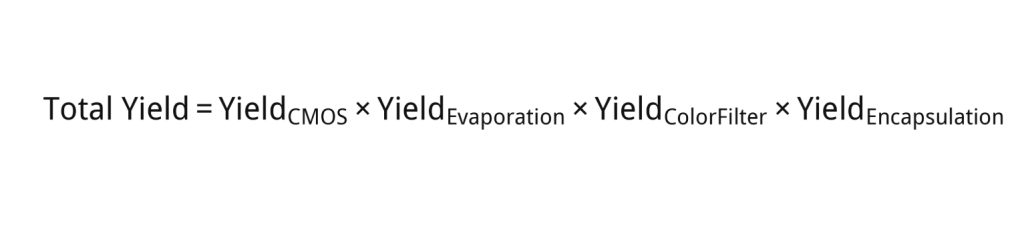
- Errors at any layer compound across the manufacturing chain [1].
3. Global Supply Chain & Integrated Solutions Landscape
Building a near-eye optical system involves more than sourcing a raw panel. Enterprise clients must combine Micro-OLED screens, specialized driving electronics, custom optics (Pancake or Waveguide), and mechanical housing [3], [4].
Global Micro-OLED Ecosystem Dynamics
┌────────────────────────────────────────────────────────────────────────┐
│                        CMOS Wafer Foundries                            │
│                  (TSMC, SMIC, Huahong Semiconductor)                   │
└───────────────────────────────────┬────────────────────────────────────┘
                                    │
                                    ▼
┌────────────────────────────────────────────────────────────────────────┐
│                      Micro-OLED Panel Producers                        │
│                (Sony, SeeYA, BOE, Kopin, Samsung/eMagin)               │
└───────────────────────────────────┬────────────────────────────────────┘
                                    │
                                    ▼
┌────────────────────────────────────────────────────────────────────────┐
│              Supply Chain Integrators & Solution Providers             │
│            (e.g., Shenzhen Pengsheng MicroVision Technology)               │
│  • Micro-OLED Displays (0.23", 0.39", 0.55", 0.71", 1.31")             │
│  • Optics Matching (Pancake, Waveguide, Eyepiece Modules)              │
│  • Custom Driver/Test Boards (MIPI, LVDS, Evaluation Kits)             │
│  • Wafer-Level Customization & Turnkey Supply Chain Management         │
└───────────────────────────────────┬────────────────────────────────────┘
                                    │
                                    ▼
┌────────────────────────────────────────────────────────────────────────┐
│                             Enterprise OEMs                            │
│      (AR/VR Headsets, Medical Imaging, Night Vision, Thermal Optics)    │
└────────────────────────────────────────────────────────────────────────┘
1. Panel Manufacturer Market Share
Global volume shipments of silicon-based OLED panels for near-eye applications remain concentrated [1], [5]:
- Sony Corporation: Leads in premium digital camera EVFs and high-tier MR headsets, leveraging deep semiconductor and optical engineering roots [1].
- SeeYA Technology : Operates 12-inch OLEDoS production lines, driving volume adoption in consumer AR/VR and industrial near-eye applications [1], [5].
- BOE & Global Players: BOE, Kopin, and Samsung Display (via eMagin acquisition) are expanding capacity, broadening choices for display buyers [1].
2. Streamlining Integration: The Role of Specialized Solution Providers
For OEMs in medical visualization, industrial inspection, thermal optics, and defense systems, dealing directly with tier-1 panel foundries can create integration hurdles—such as strict Minimum Order Quantities (MOQs), complex driver development, and optical alignment risks [3].
This gap is bridged by supply chain integration specialists like Shenzhen Pengsheng MicroVision Technology Co., Ltd.[3]. Rather than acting solely as a component distributor, specialized integrators provide end-to-end display ecosystem support [3]:
- Standard & Custom Panel Portfolio: Supplying Micro-OLED displays in key industrial form factors, including 0.23-inch, 0.39-inch, 0.55-inch, 0.71-inch, and 1.31-inch diagonal sizes, spanning high-brightness, full-color, and low-power configurations [3].
- Near-Eye Optical Module Integration: Pairing OLEDoS displays with optimized optical sub-assemblies—such as diffractive waveguides, Pancake optics, and high-resolution eyepiece modules—to ensure optimal eye-relief and modulation transfer function (MTF) performance [3], [4].
- Wafer Customization & Driver Support: Assisting enterprise clients with upstream silicon wafer customization (pixel structure, custom IC drive logic) alongside hardware development tools including MIPI/LVDS driver boards, evaluation kits, and rapid test boards [3].
- Full Supply Chain Risk Management: Consolidating silicon wafer sourcing, screen fabrication, optical assembly, and validation into a unified workflow, lowering R&D cycle times and total project BOM overhead for commercial clients [3].
4. Industry Roadmap: Cost Reduction and Future Outlook
To bring Micro-OLED BOM costs down from 30–40 per unit to consumer-friendly price points below 15–20 USD, the microdisplay industry is pursuing three primary technological shifts [1]:
- Transition to 12-inch Wafer Production Lines: Moving from 8-inch to 12-inch CMOS lines increases usable die yield per wafer by approximately 2.25 times [1]. Advanced 55 nm /40 nm logic nodes allow smaller drive circuits, reducing overall die footprint [1].
- Direct RGB Emission (Patterned OLED): Replacing the WOLED + CF structure with Direct Emission RGB (via fine metal mask or maskless photolithography) eliminates color filter light loss [4]. This boosts luminance by up to 300 – 500%, reducing power consumption, thermal load, and system battery requirements [4].
- Coexistence with Micro-LED in Ultra-Bright Optics: While Micro-OLED dominates VR, MR, and enclosed optical viewfinders [1], inorganic Micro-LED (LEDoS) will serve outdoor AR applications requiring extreme ambient light pass-through (10,000+ nits to the eye) as mass transfer techniques mature over the next 3 to 5 years [3], [6].
Authoritative References
[1] Omdia Research. Near Eye Display for XR Application Report & Display Dynamics Tracker, 2024–2026.
[2] IEEE Xplore / IEEE Transactions on Electron Devices. Silicon-Based Micro-OLED Display Architecture and CMOS Backplate Design Methodology, 2024–2025.
[3] Shenzhen Pengsheng MicroVision Technology Co., Ltd. Technical Briefing. Micro-OLED Display Modules, Wafer Customization, and Near-Eye Optical Integration Specifications, 2025–2026.
[4] Society for Information Display (SID) Symposium Digest. Advancements in Tandem WOLED Architectures and Color Filter Arrays for OLEDoS Microdisplays, 2024–2025.
[5] Yole Group. Displays & Optics for AR/VR HMDs Industry and Market Report, 2024–2025.
[6] Journal of the Society for Information Display (JSID). Comparative Analysis of Micro-OLED and Micro-LED Technologies for Next-Generation Spatial Computing, 2025.
Disclaimer
- Commercial & Informational Nature: This document is provided strictly for academic analysis, supply chain evaluation, and engineering discussion. Mention of specific brands, companies (e.g., Sony, SeeYA, BOE, Augmedics, Brainlab, Shenzhen Pengsheng MicroVision Technology Co., Ltd.), or product model sizes does not constitute a direct endorsement or endorsement warranty.
- Technical Specifications: Micro-OLED pricing, yield curves, wafer costs, and performance metrics reflect industry averages and projections derived from market research reports and technical publications. Actual project quotations and technical performance depend on custom configuration requirements and vendor agreements.