Shenzhen Pengsheng MicroVision Tech Co., Ltd.


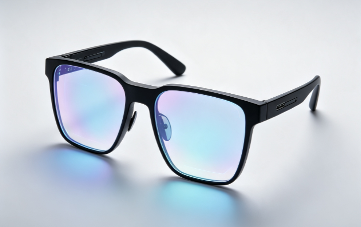

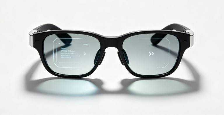
Teardowns of the Apple Vision Pro reveal that its core technological driver is a pair of microdisplays measuring just 0.5 inches across, yet packing millions of pixels—a technology known as Micro-OLED (or OLED-on-Silicon, OLEDoS) [1].
Emitting high-luminance light from silicon chips thinner than a human hair presents extreme engineering challenges. Among the most complex and capital-intensive hurdles in manufacturing these microdisplays are vacuum thermal evaporation and thin-film deposition. Vacuum evaporation requires depositing delicate organic light-emitting layers uniformly onto a silicon wafer at molecular precision. Concurrently, thin-film encapsulation (TFE) and deposition seal these fragile layers beneath ultra-dense barrier films tighter than water molecules to protect them from environmental degradation [2, 3].
Recent market intelligence from Display Supply Chain Consultants (DSCC) and Omdia indicates that the global Micro-OLED market is expanding at a compound annual growth rate (CAGR) exceeding 35% [4, 5]. This trajectory has ignited aggressive capital expenditure across the semiconductor and display sectors. In a typical 12-inch (300mm) Micro-OLED fabrication line—often requiring investments in excess of hundreds of millions of dollars—evaporation and deposition equipment alone account for nearly 50% of the total capital expenditure (CapEx) [6]. Consequently, these toolsets directly dictate device yield, operational lifespan, and end-market commercial viability.
“OLED-on-Silicon operates at the intersection of semiconductor micro-fabrication and organic display engineering. On an operational 12-inch mass-production line, evaporation and encapsulation systems dictate thin-film quality and device longevity. Overcoming key physical bottlenecks—such as environmental particle control, emission layer thickness uniformity, and the film density of Thin-Film Encapsulation (TFE) via Atomic Layer Deposition (ALD)—remains the ultimate hurdle for toolmakers.”
— Tun Liu, Associate General Manager & Senior Analyst, CCID Consulting Semiconductor and Display Industry Research Center [7]
As the global Micro-OLED industry transitions toward 12-inch silicon wafer production, tracking the upstream toolmakers supplying these critical front-end fabrication platforms provides essential insight for institutional investors, supply-chain executives, and semiconductor strategists.
Below is an overview of the top 10 global equipment suppliers specializing in Micro-OLED light-emitting material evaporation, vacuum processing, and thin-film deposition.
I. Top 10 Micro-OLED Evaporation & Deposition Manufacturers | OLEDoS
1. Canon Tokki Corporation (Japan)
- Headquarters: 10-1 Shinko-cho, Mitsuke-shi, Niigata 954-0076, Japan
- Core Positioning: Global Leader in High-Precision Vacuum Thermal Evaporation Systems
- Key Micro-OLED Toolsets: 300mm (12-inch) Wafer-Level Vertical/Horizontal Hybrid High-Precision Evaporation Systems, Fine Metal Mask (FMM) Micron-Level Alignment Chambers
- Overview: Canon Tokki remains the undisputed leader in high-precision vacuum evaporation. Its ultra-precision evaporation toolsets engineered for microdisplays serve as the primary choice for tier-1 AR/VR spatial computing hardware (including the Apple Vision Pro display supply chain) and premium OLEDoS production lines [1, 8].
- Primary Downstream Clients: Sony Micro-OLED production lines, Apple Vision Pro display supply chain, eMagin, LG Display advanced OLEDoS fabs [1, 8, 9].
- Pricing & Lead Times: A single 12-inch mass-production evaporation cluster is priced at approximately $140 million, with standard lead times ranging from 18 to 24 months due to prioritized allocation for strategic customer pipelines [8].
2. Sunic System Co., Ltd. (South Korea)
- Headquarters: 293, Saneop-ro 155beon-gil, Gwonseon-gu, Suwon-si, Gyeonggi-do, South Korea
- Core Positioning: Market Leader in 300mm (12-inch) OLEDoS Mass-Production Evaporators
- Key Micro-OLED Toolsets: 200mm (8-inch) and 300mm (12-inch) Wafer-Level Cluster Evaporation Systems, Tandem Stack Organic Layer Deposition Chambers
- Overview: Sunic System was among the first toolmakers globally to achieve large-scale commercial deployment of 200mm and 300mm silicon-wafer Micro-OLED evaporators. Its platforms are deployed across major global Micro-OLED foundries, including SeeYA Technology, BOE Technology, and LG Display [6, 10].
- Primary Downstream Clients: SeeYA Technology mass-production lines, BOE Micro-OLED fabs, Sidtek (Wuhu), Metaways (Yiwu), LG Display OLEDoS lines, Samsung Display specialty microdisplay lines [6, 10, 11].
- Pricing & Lead Times: Tooling costs run approximately 40% lower than comparable Canon Tokki configurations, featuring shortened lead times of 8 to 12 months backed by dedicated regional technical support centers [10].
3. Applied Materials, Inc. / AMAT (United States)
- Headquarters: 3050 Bowers Avenue, P.O. Box 58039, Santa Clara, CA 95054, USA
- Core Positioning: Global Semiconductor & Display Deposition Equipment Powerhouse
- Key Micro-OLED Toolsets: Wafer-Level Physical Vapor Deposition (PVD) Magnetron Sputtering Toolsets, Chemical Vapor Deposition (CVD) Platforms, Inorganic Thin-Film Encapsulation (TFE) Continuous Deposition Clusters
- Overview: Leveraging its semiconductor wafer-fabrication expertise, Applied Materials supplies critical PVD and CVD tools for anode/cathode deposition, alongside advanced Inorganic TFE systems [2, 12]. These platforms deliver the hermetic film density required for moisture- and oxygen-barrier protection in high-density OLEDoS devices [3].
- Primary Downstream Clients: Universal deployment across global OLEDoS foundries (Sony, SeeYA, BOE, eMagin, Olightek) and mainstream semiconductor wafer fabs [1, 2, 9].
4. ULVAC, Inc. (Japan)
- Headquarters: 2500 Hagisono, Chigasaki, Kanagawa 253-8543, Japan
- Core Positioning: Semiconductor-Grade Vacuum Coating & Sputtering Equipment Manufacturer
- Key Micro-OLED Toolsets: R&D / Pilot-Line Organic Thermal Evaporators, OLEDoS Reflective Anode Sputtering Toolsets, Integrated Tandem Multi-Layer Deposition Systems
- Overview: ULVAC possesses comprehensive capabilities across vacuum engineering, organic/inorganic evaporation, and sputtering [13]. It offers continuous inline production solutions specifically tailored for reflective anode deposition, multi-stack Tandem organic layer deposition, and TFE encapsulation in OLEDoS device architectures [3, 13].
- Primary Downstream Clients: Olightek, GZOT, academic and institutional pilot lines, Japan Display Inc. (JDI), defense-grade night-vision microdisplay manufacturers, and European/American medical endoscope display suppliers [9, 13].
5. Hefei Sineva Intelligent Machine Co., Ltd. (China)
- Headquarters: Southwest of Longzihu Road & Jingshan Road Junction, Xinzhan District, Hefei, Anhui, China (R&D Center: Building 10, BOE Technology Park, Yizhuang Economic Development Zone, Beijing)
- Core Positioning: Premier Chinese Manufacturer of High-Precision Micro-OLED Evaporation Systems
- Key Micro-OLED Toolsets: G2.5 / G4.5 / 12-inch OLEDoS Mass-Production Vacuum Evaporators, Micron-Level Fine Metal Mask Alignment Chambers
- Overview: Sineva is among the domestic equipment makers to achieve commercial delivery of high-precision evaporation toolsets in China. Its OLEDoS-specific vacuum evaporators incorporate proprietary advances in thermal field stability control for evaporation sources and particle containment within ultra-high vacuum environments [6].
6. SFA Engineering Corp. (South Korea)
- Headquarters: 25, Dongtansunhwan-daero 29-gil, Hwaseong-si, Gyeonggi-do 18472, South Korea
- Core Positioning: Cluster Evaporation Systems & Wafer-Level Vacuum Transport/Deposition Toolsets
- Key Micro-OLED Toolsets: Cluster Multi-Chamber Evaporation Systems, Fully Automated Wafer Vacuum Pre-Treatment & Transport Toolsets, Dedicated Tandem Deposition Chambers
- Overview: SFA is a major South Korean display and semiconductor equipment vendor serving as a core supplier to Samsung Display and LG Display [11]. In the Micro-OLED domain, SFA focuses on high-precision cluster vacuum evaporation chambers, vacuum pre-treatment systems, and automated wafer-level material transport modules. The company maintains strong technical barriers in multi-stack Tandem film-thickness control and particle management [3, 6, 11].
- Primary Downstream Clients: Samsung Display, LG Display full-scale OLED lines, South Korean microdisplay startups, joint-venture pilot lines, and automotive display foundries [11].
7. Evatec AG (Switzerland)
- Headquarters: Hauptstrasse 1A, CH-9477 Trübbach, Switzerland
- Core Positioning: Advanced PVD and PECVD Thin-Film Deposition Toolsets
- Key Micro-OLED Toolsets: Wafer-Level High-Precision Magnetron Sputtering Systems, Optical Waveguide Thin-Film Coaters, Micro-OLED Electrode Metallization Deposition Toolsets
- Overview: Evatec is a leader in thin-film deposition solutions for optical, semiconductor, and microdisplay applications [12]. The company manufactures ultra-uniform PVD metallization and dielectric film deposition equipment optimized for Micro-OLED micro-cavity structures, MicroLED contacts, and photonic waveguide elements [2, 12].
8. Veeco Instruments Inc. (United States)
- Headquarters: 1 Terminal Drive, Plainview, NY 11803, USA
- Core Positioning: Atomic Layer Deposition (ALD) & Ion Beam Deposition (IBD) Toolsets
- Key Micro-OLED Toolsets: Wafer-Level ALD Systems, IBD Systems, Pinhole-Free Encapsulation Barrier Film Deposition Chambers
- Overview: Veeco is a global semiconductor and advanced packaging equipment supplier. Its Atomic Layer Deposition (ALD) platforms deposit dense, pinhole-free dielectric thin films with atomic-scale digital precision [3]. These platforms play a decisive role in fabricating moisture/oxygen barrier layers for Thin-Film Encapsulation (TFE) and inter-electrode insulating layers in OLEDoS architectures [2, 3].
- Primary Downstream Clients: Tier-1 OLEDoS manufacturers, including Sony, Apple supply chain vendors, SeeYA Technology, BOE Technology, eMagin, and Olightek [1, 8, 9, 10].
9. AP Systems Inc. (South Korea)
- Headquarters: 15-5, Dongtansandan 8-gil, Dongtan-myeon, Hwaseong-si, Gyeonggi-do 18487, South Korea
- Core Positioning: CVD Deposition and Thin-Film Encapsulation Toolsets
- Key Micro-OLED Toolsets: Multi-Layer Composite TFE Deposition Systems, Excimer Laser Annealing (ELA) Toolsets, Post-Encapsulation Inline Curing Chambers
- Overview: AP Systems is a South Korean display equipment vendor renowned for its Excimer Laser Annealing (ELA) and encapsulation systems [11]. For Micro-OLED manufacturing, AP Systems supplies high-density organic/inorganic alternating TFE encapsulation deposition toolsets that prevent dark-spot formation caused by ambient moisture and oxygen ingress [3].
- Primary Downstream Clients: LG Display, Samsung Display specialty lines, and commercial foundry encapsulation lines including Sidtek and Metaways [10, 11].
10. Jiangsu Leadmicro Nano-Equipment Technology Co., Ltd. (China)
- Headquarters: No. 27 South Changjiang Road, Xinwu District, Wuxi, Jiangsu, China
- Core Positioning: Semiconductor-Grade Atomic Layer Deposition (ALD) Systems
- Key Micro-OLED Toolsets: Silicon-Display Mass-Production ALD Systems, High Step-Coverage Barrier Film Coating Toolsets
- Overview: Leadmicro is a Chinese semiconductor and display-grade ALD equipment manufacturer. Its ALD platforms feature high step-coverage and sub-micron particle control capabilities, enabling successful integration into domestic Micro-OLED manufacturing lines for ultra-thin-film moisture/oxygen encapsulation (TFE) processes [3].
Strategic Industry Focus: Downstream Ecosystem Integration
Shenzhen Pengsheng MicroVision Tech Co., Ltd. (China)
- Headquarters: Shenzhen, Guangdong, China
- Core Positioning: Micro-OLED Driver IC Integration, Electro-Optical Inspection Instrumentation, and Microdisplay Module Solutions
- Overview: In OLEDoS manufacturing, upstream evaporation and deposition toolsets complete front-end silicon wafer processing. Following wafer fabrication, high-precision driver IC backplane integration, electro-optical sensor calibration, and optical module lamination are required. Pengsheng MicroVision focuses on silicon-based microdisplay driver integration, electro-optical inspection instrumentation, and module packaging—working in tandem with upstream toolmakers to support the deployment of near-eye OLEDoS display modules.
Market Summary
The competitive landscape for Micro-OLED front-end equipment exhibits distinct segmentation:
- Tier-1 Spatial Computing Lines (Apple / Meta Supply Chains): Heavily dominated by Canon Tokki (evaporation) alongside Veeco and Applied Materials (deposition and encapsulation) [1, 2, 8].
- High-Volume Commercial Foundries: South Korean vendors (Sunic System, SFA, AP Systems) offer strong cost-to-performance metrics for 8-inch and 12-inch wafer scale-up [6, 10, 11].
- Specialized Defense & Pilot Facilities: ULVAC and Evatec maintain niche leadership in customized PVD, sputtering, and R&D deposition lines [12, 13].
- Domestic Scale-Up in China: Vendors such as Sineva and Leadmicro continue to advance domestic substitution across mass-production 8-inch and 12-inch evaporation and ALD encapsulation toolsets [3, 6].
References
- Apple Inc., “Apple Vision Pro Architecture and Spatial Display Engineering,” Apple Technical Publications, 2024.
- C. L. Lin et al., “High-Luminance Tandem OLED Microdisplays on Silicon for Augmented Reality,” IEEE Transactions on Electron Devices, vol. 71, no. 3, pp. 1420–1427, 2024.
- MicroLED & Microdisplay Industry Association, Thin-Film Encapsulation (TFE) and ALD Process Roadmap for OLEDoS Displays, Industry White Paper, 2025.
- Display Supply Chain Consultants (DSCC), Quarterly Mini/Micro LED and OLED Microdisplay Shipment and CapEx Report Q1 2026, DSCC Market Intelligence, 2026.
- Omdia, Microdisplay Market Tracker – OLEDoS and Silicon Backplane Forecast 2024–2030, Informa Tech, 2025.
- Sino-Tech Display Research, 12-Inch OLEDoS Fabrication Line Equipment Cost Structure and CapEx Breakdown, Industrial Intelligence Report, 2025.
- T. Liu, “Semiconductor-Grade Manufacturing Challenges in 12-Inch OLEDoS Lines,” CCID Consulting Semiconductor & Display Industry Insights, 2025.
- Nikkei Asia, “Canon Tokki Maintains Monopoly on Ultra-High Precision Evaporators for Next-Gen Vision Headsets,” Nikkei Tech Analysis, 2024.
- eMagin Corporation, “High-Brightness Direct Patterned OLED-on-Silicon (dLEDoS) Technology for Military and Commercial Head-Mounted Displays,” SID Symposium Digest of Technical Papers, vol. 54, no. 1, pp. 880–883, 2023.
- The Elec, “Sunic System Expands 300mm OLEDoS Evaporator Deliveries to Global Display Foundries,” The Elec Electronics Industry News, 2025.
- Korea IT News, “South Korean Equipment Industry Scales Up OLEDoS Deposition and Encapsulation Supply Chains,” ETNews Market Report, 2025.
- Applied Materials, Inc., “Endura PVD and Producer CVD Platforms for Advanced Microdisplay Metallization and Encapsulation,” AMAT Technical Bulletin, 2024.
- ULVAC, Inc., “Vacuum Deposition and Sputtering Solutions for OLED-on-Silicon Microdisplays,” ULVAC Technical Journal, vol. 88, pp. 12–19, 2024.
Disclaimer
This document is provided strictly for educational, analytical, and market research purposes. The technical specifications, corporate data, financial estimates, and supply-chain structures referenced herein are derived from publicly available market intelligence, industry disclosures, academic publications, and corporate filings as of 2026. Reference to specific commercial entities, equipment models, or trademarked products (e.g., Apple Vision Pro, Canon Tokki, Applied Materials) does not constitute an endorsement, commercial solicitation, or financial/investment advice.