Shenzhen Pengsheng MicroVision Tech Co., Ltd.




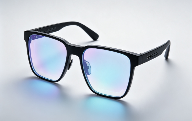
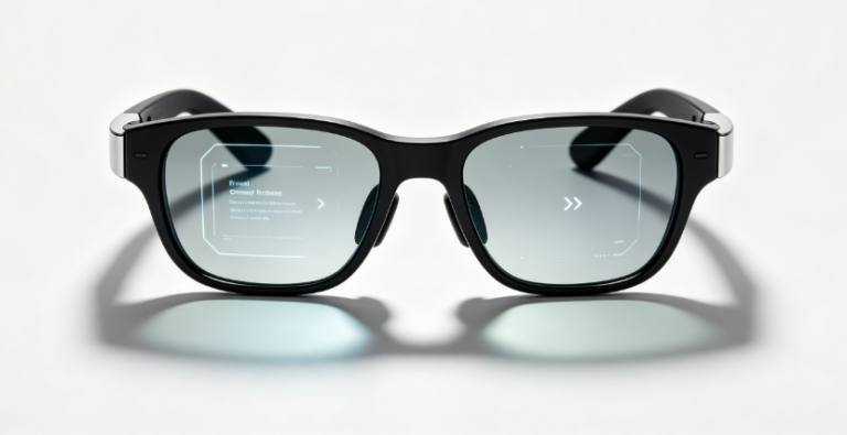
Microdisplay solutions play a pivotal role across a wide spectrum of applications, including spatial computing headsets (MR/VR), AR video/gaming glasses, smart AR glasses, outdoor tactical scopes, and FPV drone goggles [1].
In AR/VR (XR) hardware engineering, however, microdisplays represent a critical subsystem tightly integrated across optical, mechanical, electrical, and thermal domains [2].
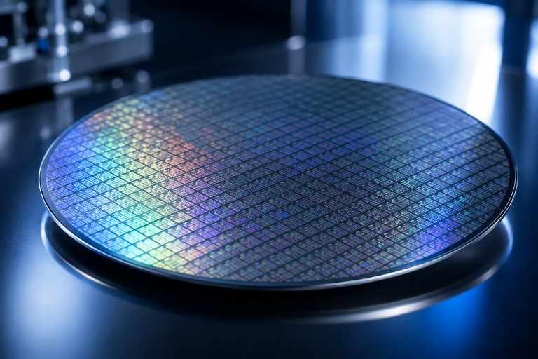
Given the extreme pixel density of silicon-based displays (PPI> 3000) and the complexity of optical pairing, any major architectural decision carries significant risk for OEMs striving for seamless technical execution and supply chain deployment. Consequently, back-calculating optical metrics, decoupling hardware from software, conducting rapid EVK (Evaluation Kit) validation, and choosing the right supply chain model are vital steps toward successful mass production.
Below is a standardized implementation framework for AR/VR OEMs to streamline microdisplay integration and supply chain sourcing.
I. Reverse Optical Engine Metric Derivation (Back-Calculating Parameters)
Rather than selecting displays solely based on standalone specification sheets, engineering teams should derive panel parameters backward from the target end-user visual experience [3].
Pengsheng MicroVision recommends utilizing the calculation logic and optical pairing rules in the tables below to complete preliminary requirement definitions:
1. Luminance Margin Calculation & Optical Matching [6]
Required Panel Luminance = Target Eye-Level Luminance/Optical Module Efficiency
| Optical Module Type | Optical Efficiency | Target Eye Luminance | Required Panel Luminance | Recommended Display Solution |
AR Array / Diffractive Waveguide [7] |
0.1% – 1% | 1,000 nits | 100,000 – 1,000,000 nits | Micro LED or RGB Direct-Emissive OLEDoS |
VR / MR Pancake Optics [6] |
10%- 15% | 300 nits | 2,000 – 3,000 nits | Tandem Micro OLED (e.g., 1.31” 4K |
| Eyepiece / Birdbath Optics | 20% – 30% | 500 nits | 2,000 – 5,000 nits | Full-Color Micro OLED (e.g., 0.39” / 0.71”) |
2. Resolution & PPD Matching Criteria [3]
| Parameter Dimension | Target Specification & Design Logic | Pengsheng MicroVision Recommended Panel Options |
| Angular Resolution (PPD) |
PPD ≥ 30 – 60 (Near-retina display experience) |
• 0.23” / 0.39” Micro OLED (Lightweight AR / Scopes) • 0.55” / 0.71” Micro OLED (AR Displays / Industrial Viewfinders) |
| Target Field of View (FOV) | Derive pixel array and panel size based on target FOV & PPD | • 1.31” 4\K Micro OLED (Immersive VR/MR Spatial Headsets) |
II. Rapid EVK Validation & Prototyping
Before committing to NRE tooling or finalizing mainboard PCB layouts, engineering teams must undergo rapid turn-on testing and optical path validation using Evaluation Kits (EVKs) to avoid costly mainboard respins [4].
- Procure Full-Featured EVKs:Request or source EVKs equipped with driver bridge ICs (e.g., Type-C/HDMI to MIPI/eDP) from solution providers. Pengsheng MicroVision offers dedicated Driver Boards & Evaluation Kits across its entire lineup of Micro OLED displays (0.23” – 1.31”) for plug-and-play debugging.
- Three Key Closed-Loop Validations:
- Optical Compatibility: Mount the display onto mock optical structures to evaluate Eye Box size, edge distortion, and chromatic aberration.
- Color & Gamut Calibration: Validate the driver IC’s Gamma adjustment capabilities and Color Look-Up Table (LUT) programming mechanisms.
- Thermal & Power Profiling: Silicon-based OLEDoS driver backplanes generate highly concentrated heat. Real-world testing of temperature curves and power draw under full luminance is essential.
III. Supply Chain Sourcing Strategy: Direct Foundry vs. Solution Provider
Select the optimal integration path based on internal engineering resources and target shipment volumes [9], [10]:
| Evaluation Matrix | Option A: Direct Foundry / Panel Maker | Option B: Supply Chain Solution Provider |
| Target OEM Profile | Tier-1 brands with dedicated hardware/optical teams, annual shipments > 100 units | Emerging teams, rapid prototyping, limited resources, annual shipments < 50 units or custom projects |
| Deliverables | Bare displays / wafers (OEM sources packaging, testing, modules, driver electronics, and optical pairing) | Turnkey Modules (Display panel + Optical module + Driver board + Firmware) |
| NRE & MOQ Thresholds | Extremely high (Costly Mask fees, minimum order quantities of thousands of wafers) | Low / Flexible for engineering samples & low-volume prototyping |
| Technical Support Depth | Limited to display hardware & register configurations | End-to-end optimization across optical, mechanical, electrical, and firmware domains |
| Wafer Customization | Requires in-house Fabless IC design capabilities | Offers upstream silicon resource integration, custom pixel layouts & ASIC drivers |
IV. Overcoming Four Key Engineering Challenges in “Optical-Mechanical-Electrical-Thermal” Integration
- Thermal Architecture:Operating temperatures above 60°C accelerate organic layer degradation in Micro OLEDs and cause color shifts
[6]. Thermal designs should incorporate ultra-thin graphene or copper heat spreaders on the back of the silicon substrate, coupled with thermal interface materials to the metal mid-frame of the glasses/headset. - Binning & Binocular Consistency (L/R Calibration):Left and right display panels must undergo rigorous Mura correction and color/luminance binning. Pengsheng MicroVision delivers near-eye display modules with pre-paired panel calibration services to prevent binocular rivalry and visual fatigue.
- Signal Integrity & FPC Routing:High-speed MIPI signals for ultra-high resolutions (e.g., 4K) are highly susceptible to EMI on compact flexible printed circuits (FPCs)
[8]. Stackup impedance and shielding design must be jointly reviewed with the display vendor. - Structural Alignment & Stress Management:Microdisplays are extremely compact (e.g., 0.23”- 0.39”), where micron-level mechanical shifts alter optical axes. Encapsulation requires high-precision dispensing and stress-relief structures to prevent adhesive curing forces from straining the underlying silicon wafer.
V. Upstream Wafer Customization, Production Quality Control & Risk Mitigation
- Upstream Wafer Customization:For deep customization projects with non-standard interfaces, custom aspect ratios, or ultra-high luminance requirements, Pengsheng MicroVision leverages upstream wafer integration capabilities to manage CMOS driver design, ASIC tape-outs, and wafer encapsulation
[8]. - Front-Load Automated Testing (ATE / Optical Jigs):During the New Product Introduction (NPI) phase, co-define automated optical test standards with solution providers to validate luminance, color uniformity, pixel defects, and FOV distortion early
[5]. - Second-Source Planning:Display driver ICs and optical elements are vulnerable to single-source risks. Hardware engineers should design PCB layouts with pin-to-pin compatible footprints for mainstream bridge ICs (e.g., Toshiba, Lattice, or domestic alternatives).
📌 About Pengsheng MicroVision
Shenzhen Pengsheng MicroVision Technology Co., Ltd. is a supply chain integrator specializing in Micro OLED Displays | Optical Modules | Wafer Customization | Integrated Display Solutions.
We are dedicated to providing one-stop technical support for global AR/VR, near-eye display, medical equipment, night-vision scopes, and industrial inspection customers:
- Comprehensive Micro OLED Lineup: Full range of screen sizes (0.23” / 0.39” / 0.55” / 0.71” / 1.31”);
- Optical Module Pairing: System integration of Micro OLED with Waveguide, Pancake, and Eyepiece optical systems;
- Turnkey Evaluation Support: Driver boards, Evaluation Kits (EVKs), display bring-up solutions, and end-to-end supply chain management.
References
[1] Omdia Research. Display Dynamics – Rapid Decline in OLEDoS Display Prices Set to Accelerate Market Growth. Informa Tech, 2024–2026.
[2] Yole Intelligence. Status of the Display Industry & Microdisplays Report. Yole Group, 2025.
[3] TrendForce. TrendForce Micro OLED & Near-Eye Display Market Analysis. TrendForce Press Center, 2025–2026.
[4] OLED-Info. OLED Microdisplays Industry & Global Supplier Directory. OLED-Info Portal, 2026.
[5] Mordor Intelligence. OLED Microdisplay Market – Size, Trends, Share & Growth Forecasts (2026–2031). Mordor Intelligence Reports, 2026.
[6] Society for Information Display (SID). Journal of the Society for Information Display (JSID) – High-PPI Silicon Backplanes and OLEDoS Manufacturing Advances, 2025.
[7] SPIE Digital Library. Proceedings of SPIE: Organic Light-Emitting Diodes and Near-Eye Optical Systems Architecture, 2024–2026.
[8] IEEE Xplore. IEEE Transactions on Electron Devices – Native RGB OLEDoS Direct Emission Technologies for AR Microdisplays, 2025.
[9] Display Daily. Next-Generation XR Displays: Open-Foundry Models and Micro OLED Scaling, Display Daily Publications, 2025.
[10] GII Research. Global OLED Microdisplay Market Share Analysis and Supply Chain Report (2025–2030). GII, 2025.
Disclaimer
- Information Purpose: Technical parameters, derivation formulas, and market analysis data contained herein are intended solely for engineering selection, academic exchange, and R&D reference. They do not constitute official factory acceptance criteria or statutory testing standards.
- Intellectual Property & Trademarks: All third-party market research reports (e.g., Omdia, Yole, TrendForce, SID, SPIE, IEEE) and company/brand names referenced in this document remain the intellectual property and registered trademarks of their respective owners. Their inclusion is purely for objective industry analysis and does not imply direct endorsement or exclusive affiliation.
- Specification Variations: Real-world performance of microdisplay panels (Micro OLED / Micro LED), optical modules, and driver electronics may vary depending on panel batch variations, encapsulation processes, thermal environments, and firmware revisions. For formal project procurement and engineering development, please refer to official Datasheets and contractual documentation issued by Shenzhen Pengsheng MicroVision Technology Co., Ltd. or designated original component manufacturers.