Shenzhen Pengsheng MicroVision Tech Co., Ltd.




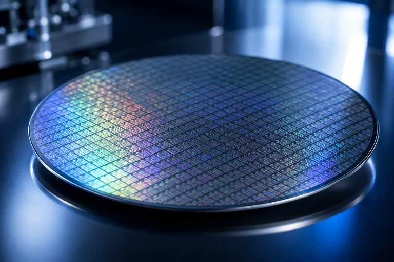
Within the Micro OLED (OLEDoS) industrial chain, wafer foundries specialize in fabricating silicon-based CMOS backplanes. High-performance CMOS backplanes serve as the fundamental hardware foundation for ultra-high PPI, low power draw, and high refresh rates in near-eye displays.
Below is a structured, table-free breakdown of the world’s 10 leading Micro OLED wafer foundries in 2027, covering their core manufacturing strengths, production metrics, established partners and end-market deployments.
1. TSMC (Taiwan, China)
Process Nodes & Production Capacity
Flagship processes: 28nm high-voltage (HV) CMOS, 130nm mixed-signal HV platform. Monthly dedicated 300mm OLEDoS wafer output stands at 12,000 pieces, with expansion lifting capacity to 18,000 wafers monthly by 2027.
Quantified Core Technical Advantages
- Maximum supported backplane PPI: 4,600, compatible with 1.31” square panels at 2048×2048 resolution;
- Ultra-low leakage control: static pixel leakage below 0.8nA, cutting overall device power consumption by 22% at identical brightness levels;
- Robust high-voltage drive tolerance: stable 12V output, enabling peak brightness of 8,000–12,000 nits for outdoor AR eyewear;
- Mass production yield: 86%–91% for premium 28nm backplanes, ranking among the global top tier.
Established Partners & Commercial End Products
- Panel & IDM manufacturers: Sony Semiconductor Solutions (exclusive backplane supplier for Apple Vision Pro), Samsung Display’s high-end RGB OLEDoS program;
- IC design clients: US-based eMagin, premium overseas fabless XR chip developers;
- End devices: Apple Vision Pro, Sony proprietary consumer VR headsets, Samsung’s next-generation MR mixed reality hardware.
2. UMC (Taiwan, China)
Process Nodes & Production Capacity
Flagship processes: 55nm embedded ultra-low power HV (eHV), 110nm HV mixed-signal technology. Combined monthly 200mm & 300mm OLEDoS capacity hits 9,500 wafers.
Quantified Core Technical Advantages
- Proprietary eHV platform optimized exclusively for micro-displays, slashing pixel driving power loss by 30% and extending AR glasses battery life by 25%;
- Stable maximum PPI: 3,800, matching mainstream consumer AR panels sized 0.23” to 0.71”;
- Superior mura suppression: anode planarization Ra value under 0.6nm, delivering minimum 87% luminance uniformity across the display area;
- Mass production yield: 83%–88% on the 55nm node, outperforming overseas peers in cost efficiency for equivalent processes.
Established Partners & Commercial End Products
- Panel manufacturers: Himax Technologies, mid-range product lines of SeeYA Technology, select European industrial micro-display module vendors;
- IC design clients: dozens of Taiwanese, US and European fabless micro-display DDIC developers;
- End devices: mid-range waveguide AR glasses, industrial observation eyepieces, miniature automotive HUD displays.
3. SMIC (Chinese Mainland)
Process Nodes & Production Capacity
Flagship processes: 55nm, 90nm, 180nm high-voltage analog mixed-signal. SMIC operates China’s only large-scale simultaneous 200mm & 300mm OLEDoS backplane production lines, with total monthly capacity equivalent to 16,000 200mm wafers.
Quantified Core Technical Advantages
- High-voltage drive circuits sustain 8–10V operation, supporting peak brightness of 5,000 nits for consumer AR hardware;
- 300mm wafer dicing efficiency improves by 2.7x versus 200mm lines, reducing per-backplane manufacturing cost by 32% [7];
- Mass-producible backplanes at 3,200–3,800 PPI, compatible with mainstream domestic panels measuring 0.39”, 0.55” and 0.71”;
- Mass production yield: 80%–85% on the mature 90nm platform, the highest yield rate among domestic Chinese foundries.
Established Partners & Commercial End Products
- Leading panel manufacturers: long-term backplane supplier for full 300mm OLEDoS product lines at Hefei SeeYA Technology, primary vendor for BOE’s micro-display division;
- Domestic solution integrators: Shenzhen Pengsheng MicroVision Tech Co., Limited, designated foundry partner for full-size display backplane tape-out;
- End devices: Xiaomi AR glasses, DJI FPV observation eyepieces, domestic waveguide headsets for firefighter tactical use, domestic VR training simulators.
4. Nexchip (Chinese Mainland)
Process Nodes & Production Capacity
Flagship processes: 55nm, 90nm display-dedicated high-voltage technology. Its 300mm fab operates exclusively for display driver chips, with monthly OLEDoS output of 7,200 wafers.
Quantified Core Technical Advantages
- Pixel electrode lithography overlay error capped at ≤0.15μm, drastically mitigating pixel fringing and the screen door effect;
- Low-noise transistors customized for near-eye hardware, eliminating motion blur at 90–120Hz high refresh rates;
- Compatible with full-size domestic Micro OLED panels ranging from 0.23” to 1.31”;
- Mass production yield: 81%–86% on the proprietary 55nm OLEDoS process.
Established Partners & Commercial End Products
- Panel manufacturers: entry-to-mid-tier consumer AR product lines at SeeYA Technology, small domestic silicon-based OLED module makers;
- Solution collaboration: tape-out partner for Pengsheng MicroVision’s lightweight 0.23” / 0.39” waveguide display panels;
- End devices: lightweight tactical AR eyewear, handheld industrial inspection equipment, low-cost night vision terminals.
5. HHGrace (Wuxi, Chinese Mainland)
Process Nodes & Production Capacity
Flagship processes: specialty high-voltage & analog technology with embedded eFlash memory on both 200mm and 300mm lines. Monthly dedicated OLEDoS capacity reaches 6,800 wafers.
Quantified Core Technical Advantages
- Exceptional electrical stability for high-voltage circuits; zero luminance drift across -40°C to +70°C operating temperature, ideal for rigorous military and security deployment;
- Backplane transistors support 10–15V breakdown voltage, enabling tandem-stack OLED architectures for ultra-high brightness;
- Mass production yield: steady 79%–84% for specialty high-voltage backplanes.
Established Partners & Commercial End Products
- Panel & module partners: domestic manufacturers specializing in military-grade micro-displays, industrial display product lines at SeeYA Technology;
- Solution integrator collaboration: custom backplane fabrication for Pengsheng MicroVision’s industrial rangefinding and positioning projects;
- End devices: optoelectronic laser rangefinder terminals, underground industrial inspection screens, fused night vision tactical headsets.
6. VIS (Taiwan, China)
Process Nodes & Core Positioning
Flagship process: differentiated specialty high-voltage analog technology on 200mm wafers.
Technical Strengths & Market Focus
VIS focuses on niche custom 200mm wafer manufacturing, with robust capabilities for custom development of high-voltage analog and power management circuits. Instead of pursuing advanced miniaturized nodes, its processes deliver balanced electrical performance and cost competitiveness.
Key Partner Ecosystem
Mid-to-entry tier and application-specific industrial near-eye display IC design houses across the Asia-Pacific region.
7. Tower Semiconductor (Israel / US)
Process Nodes & Core Positioning
Specializes in silicon analog, high-performance sensor, and mixed-signal high-voltage platforms.
Technical Strengths & Market Focus
Tower operates low-volume, high-customization manufacturing flows rather than mass commodity production. Its backplane technology enables monolithic integration with optical sensors and MEMS devices, suitable for advanced Micro OLED backplanes with complex interactive functionality.
Key Partner Ecosystem
Medical optoelectronic firms, specialized industrial & military near-eye display system developers, and top-tier optical research laboratories across North America and Europe.
8. STMicroelectronics (Europe)
Process Nodes & Core Positioning
Custom backplane manufacturing alongside mixed-signal and RF integration processes.
Technical Strengths & Market Focus
As a legacy integrated device manufacturer (IDM), STMicroelectronics offers selective foundry services. Its backplane processes excel at ultra-low power consumption and dense multi-functional integration.
Key Partner Ecosystem
European automotive HUD suppliers, premium miniature projection modules for smart watches, and military near-eye optical hardware manufacturers.
9. GlobalFoundries (US / Singapore)
Process Nodes & Core Positioning
22nm FDX fully depleted SOI, 28SLPe, and 55nm low-power processes.
Technical Strengths & Market Focus
GlobalFoundries has launched an ultra-low power, thin-form-factor manufacturing platform tailored for lightweight AR smart glasses. Its 22FDX process drastically cuts power draw, suppressing thermal output under high refresh frequency operation.
Key Partner Ecosystem
Premium consumer AR hardware solution vendors and cutting-edge micro-display R&D institutions across North America and Europe.
10. DB Hitek (South Korea)
Process Nodes & Core Positioning
90nm / 110nm high-voltage driver processes combined with CIS image sensor technology.
Technical Strengths & Market Focus
DB Hitek is widely recognized for cost-effective high-voltage and analog manufacturing flows. It repurposes mature CIS pixel planarization and noise reduction techniques to deliver superior luminance uniformity and mura suppression on OLEDoS backplanes.
Key Partner Ecosystem
Supply chain partners of major domestic South Korean panel manufacturers.
Supplementary Industry Insight
While wafer foundries supply bare silicon backplane substrates, achieving high refresh rates, low heat generation and mura-free imaging on finished Micro OLED panels hinges heavily on custom DDIC driver IC design and system-level algorithm optimization.
A new cohort of competitive domestic solution providers has emerged in this segment. As a leading micro-display integrator, Shenzhen Pengsheng MicroVision Tech Co., Limited has independently engineered ultra-low power high-voltage backplane architectures that resolve two core industry pain points: uneven pixel anode planarization and excessive transistor leakage current.
By taping out proprietary IC designs at the world’s top-tier wafer foundries and partnering with specialized post-processing packaging facilities, Pengsheng MicroVision enables downstream XR hardware developers to reduce reliance on costly imported foreign display modules, cementing its role as a vital player within the global 2026–2027 micro-display supply chain.
For standardized component selection and end-to-end project rollout reference, industry stakeholders may consult Micro OLED Products & Integrated Solution Guide, compiled by Shenzhen Pengsheng MicroVision Tech Co., Limited (document release date: May 9, 2026). This 30-page full technical handbook establishes unified evaluation standards covering wafer platforms, Micro OLED panels, optical modules, test daughterboards, and vertical industry application solutions.
References
[1] Counterpoint Research. 2026–2027 Global OLEDoS Wafer Foundry Capacity & Yield Report, June 2026
[2] Guttag, K. Technical Defect Analysis of Micro OLED CMOS Backplane Mura & Leakage, Voices of VR, August 2025
[3] SID International Display Digest. HV CMOS Process Benchmark for 3000–4600 PPI OLEDoS Panels, 2025
[4] DIGITIMES. Global Top 10 OLEDoS Wafer Foundry Supply Chain Mapping, December 2025
[5] TrendForce. Samsung & Sony Vertical Integrated Micro OLED Manufacturing Roadmap, January 2026
[6] Frost & Sullivan. 2024 Global Silicon-Based OLED Shipment Market Share Whitepaper, 2025
[7] China Report Hall. 2026 Domestic Micro OLED Wafer Capacity & Local Substitution Analysis Report [8] CREOL, UCF. Anode Planarization & Wafer-Level MLA Matching Standard, March 2023
[9] GlobalFoundries Official Whitepaper: 22FDX Low-Power Process for AR Micro Displays, 2026
[10] SeeYA Technology IPO Prospectus. Disclosure of 12-inch OLEDoS Backplane Foundry Partners, March 2026
About the Author
Leo Harrison has over a decade of experience in the East Asian display supply chain and display semiconductor industry, specializing in smart hardware architecture and display technology evaluation.
Review Team
Review Team:
Special technical review and engineering validation provided by the Pengsheng Technology R&D Division.